R0K561622S000BE Renesas Electronics America, R0K561622S000BE Datasheet - Page 26
R0K561622S000BE
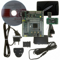
Manufacturer Part Number
R0K561622S000BE
Description
KIT STARTER FOR H8SX/1622
Manufacturer
Renesas Electronics America
Series
Renesas Starter Kits (RSK)r
Type
MCUr
Specifications of R0K561622S000BE
Contents
Board, Cables, CD, Debugger, Power Supply
Silicon Manufacturer
Renesas
Features
Coding And Debugging, E10A Emulator, RS232 Serial Connection
Kit Contents
Board
Silicon Family Name
H8SX/1622F
Silicon Core Number
R5F61622N50LGV
Lead Free Status / RoHS Status
Lead free / RoHS Compliant
For Use With/related Products
H8SX/1622
Lead Free Status / RoHS Status
Lead free / RoHS Compliant, Lead free / RoHS Compliant


Section 20 D/A Converter ................................................................................. 769
20.1
20.2
20.3
20.4
20.5
Section 21 RAM ................................................................................................ 775
Section 22 Flash Memory.................................................................................. 777
22.1
22.2
22.3
22.4
22.5
22.6
22.7
22.8
22.9
22.10 Flash Memory Emulation Using RAM............................................................................. 833
22.11 Switching between User MAT and User Boot MAT........................................................ 836
22.12 Programmer Mode ............................................................................................................ 837
22.13 Standard Serial Communication Interface Specifications for Boot Mode ........................ 837
22.14 Usage Notes ...................................................................................................................... 866
Rev. 2.00 Sep. 16, 2009 Page xxiv of xxviii
19.6.5
Features............................................................................................................................. 769
Input/Output Pins.............................................................................................................. 770
Register Descriptions........................................................................................................ 770
20.3.1
20.3.2
Operation .......................................................................................................................... 773
Usage Notes ...................................................................................................................... 774
20.5.1
20.5.2
Features............................................................................................................................. 777
Mode Transition Diagram................................................................................................. 779
Memory MAT Configuration ........................................................................................... 781
Block Structure ................................................................................................................. 782
Programming/Erasing Interface ........................................................................................ 783
Input/Output Pins.............................................................................................................. 785
Register Descriptions........................................................................................................ 785
22.7.1
22.7.2
22.7.3
On-Board Programming Mode ......................................................................................... 806
22.8.1
22.8.2
22.8.3
22.8.4
Protection.......................................................................................................................... 830
22.9.1
22.9.2
22.9.3
DSE Bit............................................................................................................. 768
D/A Data Registers 0 and 1 (DADR0 and DADR1)......................................... 770
D/A Control Register 01 (DACR01) ................................................................ 771
Module Stop Function Setting .......................................................................... 774
D/A Output Hold Function in Software Standby Mode.................................... 774
Programming/Erasing Interface Registers ........................................................ 786
Programming/Erasing Interface Parameters ..................................................... 793
RAM Emulation Register (RAMER)................................................................ 805
Boot Mode ........................................................................................................ 806
User Program Mode.......................................................................................... 810
User Boot Mode................................................................................................ 820
On-Chip Program and Storable Area for Program Data ................................... 824
Hardware Protection ......................................................................................... 830
Software Protection........................................................................................... 831
Error Protection ................................................................................................ 831
Related parts for R0K561622S000BE
Image
Part Number
Description
Manufacturer
Datasheet
Request
R

Part Number:
Description:
KIT STARTER FOR M16C/29
Manufacturer:
Renesas Electronics America
Datasheet:

Part Number:
Description:
KIT STARTER FOR R8C/2D
Manufacturer:
Renesas Electronics America
Datasheet:

Part Number:
Description:
R0K33062P STARTER KIT
Manufacturer:
Renesas Electronics America
Datasheet:

Part Number:
Description:
KIT STARTER FOR R8C/23 E8A
Manufacturer:
Renesas Electronics America
Datasheet:

Part Number:
Description:
KIT STARTER FOR R8C/25
Manufacturer:
Renesas Electronics America
Datasheet:

Part Number:
Description:
KIT STARTER H8S2456 SHARPE DSPLY
Manufacturer:
Renesas Electronics America
Datasheet:

Part Number:
Description:
KIT STARTER FOR R8C38C
Manufacturer:
Renesas Electronics America
Datasheet:

Part Number:
Description:
KIT STARTER FOR R8C35C
Manufacturer:
Renesas Electronics America
Datasheet:

Part Number:
Description:
KIT STARTER FOR R8CL3AC+LCD APPS
Manufacturer:
Renesas Electronics America
Datasheet:
Part Number:
Description:
KIT STARTER FOR RX610
Manufacturer:
Renesas Electronics America
Datasheet:

Part Number:
Description:
KIT STARTER FOR R32C/118
Manufacturer:
Renesas Electronics America
Datasheet:

Part Number:
Description:
KIT DEV RSK-R8C/26-29
Manufacturer:
Renesas Electronics America
Datasheet:

Part Number:
Description:
KIT STARTER FOR SH7124
Manufacturer:
Renesas Electronics America
Datasheet:

Part Number:
Description:
KIT DEV FOR SH7203
Manufacturer:
Renesas Electronics America
Datasheet:
Part Number:
Description:
KIT STARTER FOR R8C/18191A1B
Manufacturer:
Renesas Electronics America
Datasheet: