R0K561622S000BE Renesas Electronics America, R0K561622S000BE Datasheet - Page 28
R0K561622S000BE
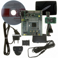
Manufacturer Part Number
R0K561622S000BE
Description
KIT STARTER FOR H8SX/1622
Manufacturer
Renesas Electronics America
Series
Renesas Starter Kits (RSK)r
Type
MCUr
Specifications of R0K561622S000BE
Contents
Board, Cables, CD, Debugger, Power Supply
Silicon Manufacturer
Renesas
Features
Coding And Debugging, E10A Emulator, RS232 Serial Connection
Kit Contents
Board
Silicon Family Name
H8SX/1622F
Silicon Core Number
R5F61622N50LGV
Lead Free Status / RoHS Status
Lead free / RoHS Compliant
For Use With/related Products
H8SX/1622
Lead Free Status / RoHS Status
Lead free / RoHS Compliant, Lead free / RoHS Compliant


24.8
24.9
24.10 Sleep Instruction Exception Handling .............................................................................. 921
24.11 Bφ Clock Output Control.................................................................................................. 924
24.12 Usage Notes ...................................................................................................................... 925
Section 25 List of Registers............................................................................... 927
25.1
25.2
25.3
Section 26 Electrical Characteristics ................................................................. 973
26.1
26.2
Rev. 2.00 Sep. 16, 2009 Page xxvi of xxviii
Deep Software Standby Mode .......................................................................................... 908
24.8.1
24.8.2
24.8.3
24.8.4
24.8.5
24.8.6
24.8.7
Hardware Standby Mode .................................................................................................. 919
24.9.1
24.9.2
24.9.3
24.9.4
24.12.1 I/O Port Status................................................................................................... 925
24.12.2 Current Consumption during Oscillation Settling Standby Period ................... 925
24.12.3 Module Stop State of DMAC or DTC .............................................................. 925
24.12.4 On-Chip Peripheral Module Interrupts ............................................................. 925
24.12.5 Writing to MSTPCRA, MSTPCRB, and MSTPCRC....................................... 925
24.12.6 Control of Input Buffers by DIRQnE (n = 3 to 0)............................................. 926
24.12.7 Input Buffer Control by DIRQnE (n = 3 to 0) .................................................. 926
24.12.8 Bφ Output State ................................................................................................ 926
Register Addresses (Address Order)................................................................................. 928
Register Bits ..................................................................................................................... 941
Register States in Each Operating Mode .......................................................................... 960
Electrical Characteristics .................................................................................................. 973
26.1.1
26.1.2
26.1.3
26.1.4
26.1.5
26.1.6
Timing Charts ................................................................................................................... 992
Setting Oscillation Settling Time after Exit from
Deep Software Standby Mode .......................................................................... 911
Entry to Deep Software Standby Mode ............................................................ 908
Exit from Deep Software Standby Mode.......................................................... 909
Pin State on Exit from Deep Software Standby Mode...................................... 910
Bφ Operation after Exit from Deep Software Standby Mode ........................... 910
Deep Software Standby Mode Application Example ....................................... 913
Flowchart of Deep Software Standby Mode Operation .................................... 917
Transition to Hardware Standby Mode............................................................. 919
Clearing Hardware Standby Mode.................................................................... 919
Hardware Standby Mode Timing...................................................................... 919
Timing Sequence at Power-On ......................................................................... 920
Absolute Maximum Ratings ............................................................................. 973
DC Characteristics ............................................................................................ 974
AC Characteristics ............................................................................................ 979
A/D Conversion Characteristics ....................................................................... 986
D/A Conversion Characteristics ....................................................................... 986
∆ΣA/D Conversion Characteristics................................................................... 987
Related parts for R0K561622S000BE
Image
Part Number
Description
Manufacturer
Datasheet
Request
R

Part Number:
Description:
KIT STARTER FOR M16C/29
Manufacturer:
Renesas Electronics America
Datasheet:

Part Number:
Description:
KIT STARTER FOR R8C/2D
Manufacturer:
Renesas Electronics America
Datasheet:

Part Number:
Description:
R0K33062P STARTER KIT
Manufacturer:
Renesas Electronics America
Datasheet:

Part Number:
Description:
KIT STARTER FOR R8C/23 E8A
Manufacturer:
Renesas Electronics America
Datasheet:

Part Number:
Description:
KIT STARTER FOR R8C/25
Manufacturer:
Renesas Electronics America
Datasheet:

Part Number:
Description:
KIT STARTER H8S2456 SHARPE DSPLY
Manufacturer:
Renesas Electronics America
Datasheet:

Part Number:
Description:
KIT STARTER FOR R8C38C
Manufacturer:
Renesas Electronics America
Datasheet:

Part Number:
Description:
KIT STARTER FOR R8C35C
Manufacturer:
Renesas Electronics America
Datasheet:

Part Number:
Description:
KIT STARTER FOR R8CL3AC+LCD APPS
Manufacturer:
Renesas Electronics America
Datasheet:
Part Number:
Description:
KIT STARTER FOR RX610
Manufacturer:
Renesas Electronics America
Datasheet:

Part Number:
Description:
KIT STARTER FOR R32C/118
Manufacturer:
Renesas Electronics America
Datasheet:

Part Number:
Description:
KIT DEV RSK-R8C/26-29
Manufacturer:
Renesas Electronics America
Datasheet:

Part Number:
Description:
KIT STARTER FOR SH7124
Manufacturer:
Renesas Electronics America
Datasheet:

Part Number:
Description:
KIT DEV FOR SH7203
Manufacturer:
Renesas Electronics America
Datasheet:
Part Number:
Description:
KIT STARTER FOR R8C/18191A1B
Manufacturer:
Renesas Electronics America
Datasheet: