R0K561622S000BE Renesas Electronics America, R0K561622S000BE Datasheet - Page 15
R0K561622S000BE
Manufacturer Part Number
R0K561622S000BE
Description
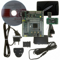
KIT STARTER FOR H8SX/1622
Manufacturer
Renesas Electronics America
Series
Renesas Starter Kits (RSK)r
Type
MCUr
Specifications of R0K561622S000BE
Contents
Board, Cables, CD, Debugger, Power Supply
Silicon Manufacturer
Renesas
Features
Coding And Debugging, E10A Emulator, RS232 Serial Connection
Kit Contents
Board
Silicon Family Name
H8SX/1622F
Silicon Core Number
R5F61622N50LGV
Lead Free Status / RoHS Status
Lead free / RoHS Compliant
For Use With/related Products
H8SX/1622
Lead Free Status / RoHS Status
Lead free / RoHS Compliant, Lead free / RoHS Compliant


8.3
8.4
8.5
8.6
8.7
8.8
8.2.6
8.2.7
8.2.8
8.2.9
8.2.10
8.2.11
8.2.12
Bus Configuration............................................................................................................. 180
Multi-Clock Function and Number of Access Cycles ...................................................... 181
External Bus...................................................................................................................... 185
8.5.1
8.5.2
8.5.3
8.5.4
8.5.5
8.5.6
Basic Bus Interface ........................................................................................................... 202
8.6.1
8.6.2
8.6.3
8.6.4
8.6.5
8.6.6
8.6.7
Byte Control SRAM Interface .......................................................................................... 215
8.7.1
8.7.2
8.7.3
8.7.4
8.7.5
8.7.6
8.7.7
8.7.8
Burst ROM Interface ........................................................................................................ 223
8.8.1
8.8.2
8.8.3
8.8.4
8.8.5
8.8.6
Idle Control Register (IDLCR) ......................................................................... 170
Bus Control Register 1 (BCR1) ........................................................................ 172
Bus Control Register 2 (BCR2) ........................................................................ 174
Endian Control Register (ENDIANCR)............................................................ 175
SRAM Mode Control Register (SRAMCR) ..................................................... 176
Burst ROM Interface Control Register (BROMCR)......................................... 177
Address/Data Multiplexed I/O Control Register (MPXCR) ............................. 179
Input/Output Pins.............................................................................................. 185
Area Division.................................................................................................... 188
Chip Select Signals ........................................................................................... 189
External Bus Interface....................................................................................... 190
Area and External Bus Interface ....................................................................... 194
Endian and Data Alignment.............................................................................. 199
Data Bus............................................................................................................ 202
I/O Pins Used for Basic Bus Interface .............................................................. 202
Basic Timing..................................................................................................... 203
Wait Control ..................................................................................................... 209
Read Strobe (RD) Timing................................................................................. 211
Extension of Chip Select (CS) Assertion Period............................................... 212
DACK Signal Output Timing ........................................................................... 214
Byte Control SRAM Space Setting................................................................... 215
Data Bus............................................................................................................ 215
I/O Pins Used for Byte Control SRAM Interface ............................................. 216
Basic Timing..................................................................................................... 217
Wait Control ..................................................................................................... 219
Read Strobe (RD).............................................................................................. 221
Extension of Chip Select (CS) Assertion Period............................................... 221
DACK Signal Output Timing ........................................................................... 221
Burst ROM Space Setting................................................................................. 223
Data Bus............................................................................................................ 223
I/O Pins Used for Burst ROM Interface............................................................ 224
Basic Timing..................................................................................................... 225
Wait Control ..................................................................................................... 227
Read Strobe (RD) Timing................................................................................. 227
Rev. 2.00 Sep. 16, 2009 Page xiii of xxviii
Related parts for R0K561622S000BE
Image
Part Number
Description
Manufacturer
Datasheet
Request
R

Part Number:
Description:
KIT STARTER FOR M16C/29
Manufacturer:
Renesas Electronics America
Datasheet:

Part Number:
Description:
KIT STARTER FOR R8C/2D
Manufacturer:
Renesas Electronics America
Datasheet:

Part Number:
Description:
R0K33062P STARTER KIT
Manufacturer:
Renesas Electronics America
Datasheet:

Part Number:
Description:
KIT STARTER FOR R8C/23 E8A
Manufacturer:
Renesas Electronics America
Datasheet:

Part Number:
Description:
KIT STARTER FOR R8C/25
Manufacturer:
Renesas Electronics America
Datasheet:

Part Number:
Description:
KIT STARTER H8S2456 SHARPE DSPLY
Manufacturer:
Renesas Electronics America
Datasheet:

Part Number:
Description:
KIT STARTER FOR R8C38C
Manufacturer:
Renesas Electronics America
Datasheet:

Part Number:
Description:
KIT STARTER FOR R8C35C
Manufacturer:
Renesas Electronics America
Datasheet:

Part Number:
Description:
KIT STARTER FOR R8CL3AC+LCD APPS
Manufacturer:
Renesas Electronics America
Datasheet:
Part Number:
Description:
KIT STARTER FOR RX610
Manufacturer:
Renesas Electronics America
Datasheet:

Part Number:
Description:
KIT STARTER FOR R32C/118
Manufacturer:
Renesas Electronics America
Datasheet:

Part Number:
Description:
KIT DEV RSK-R8C/26-29
Manufacturer:
Renesas Electronics America
Datasheet:

Part Number:
Description:
KIT STARTER FOR SH7124
Manufacturer:
Renesas Electronics America
Datasheet:

Part Number:
Description:
KIT DEV FOR SH7203
Manufacturer:
Renesas Electronics America
Datasheet:
Part Number:
Description:
KIT STARTER FOR R8C/18191A1B
Manufacturer:
Renesas Electronics America
Datasheet: