R0K561622S000BE Renesas Electronics America, R0K561622S000BE Datasheet - Page 317
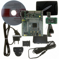
R0K561622S000BE
Manufacturer Part Number
R0K561622S000BE
Description
KIT STARTER FOR H8SX/1622
Manufacturer
Renesas Electronics America
Series
Renesas Starter Kits (RSK)r
Type
MCUr
Specifications of R0K561622S000BE
Contents
Board, Cables, CD, Debugger, Power Supply
Silicon Manufacturer
Renesas
Features
Coding And Debugging, E10A Emulator, RS232 Serial Connection
Kit Contents
Board
Silicon Family Name
H8SX/1622F
Silicon Core Number
R5F61622N50LGV
Lead Free Status / RoHS Status
Lead free / RoHS Compliant
For Use With/related Products
H8SX/1622
Lead Free Status / RoHS Status
Lead free / RoHS Compliant, Lead free / RoHS Compliant


(2)
In single address mode, data between an external device and an external memory is directly
transferred using the DACK pin instead of DSAR or DDAR. A transfer at a time is performed in
one bus cycle. In this mode, the data bus width must be the same as the data access size. For
details on the data bus width, see section 8, Bus Controller (BSC).
The DMAC accesses an external device as the transfer source or destination by outputting the
strobe signal (DACK) to the external device with DACK and accesses the other transfer target by
outputting the address. Accordingly, the DMA transfer is performed in one bus cycle. Figure 9.4
shows an example of a transfer between an external memory and an external device with the
DACK pin. In this example, the external device outputs data on the data bus and the data is written
to the external memory in the same bus cycle.
The transfer direction is decided by the DIRS bit in DACR which specifies an external device with
the DACK pin as the transfer source or destination. When DIRS = 0, data is transferred from an
external memory (DSAR) to an external device with the DACK pin. When DIRS = 1, data is
transferred from an external device with the DACK pin to an external memory (DDAR). The
settings of registers which are not used as the transfer source or destination are ignored.
The DACK signal output is enabled in single address mode by the DACKE bit in DMDR. The
DACK signal is low active.
The TEND signal output is enabled or disabled by the TENDE bit in DMDR. The TEND signal is
output in one bus cycle. When an idle cycle is inserted before the bus cycle, the TEND signal is
also output in the idle cycle.
Address B
Address T
Single Address Mode
A
A
Figure 9.3 Operations in Dual Address Mode
Transfer
Address update setting is as follows:
Source address increment
Fixed destination address
Rev. 2.00 Sep. 16, 2009 Page 287 of 1036
Section 9 DMA Controller (DMAC)
REJ09B0414-0200
Address T
B
Related parts for R0K561622S000BE
Image
Part Number
Description
Manufacturer
Datasheet
Request
R

Part Number:
Description:
KIT STARTER FOR M16C/29
Manufacturer:
Renesas Electronics America
Datasheet:

Part Number:
Description:
KIT STARTER FOR R8C/2D
Manufacturer:
Renesas Electronics America
Datasheet:

Part Number:
Description:
R0K33062P STARTER KIT
Manufacturer:
Renesas Electronics America
Datasheet:

Part Number:
Description:
KIT STARTER FOR R8C/23 E8A
Manufacturer:
Renesas Electronics America
Datasheet:

Part Number:
Description:
KIT STARTER FOR R8C/25
Manufacturer:
Renesas Electronics America
Datasheet:

Part Number:
Description:
KIT STARTER H8S2456 SHARPE DSPLY
Manufacturer:
Renesas Electronics America
Datasheet:

Part Number:
Description:
KIT STARTER FOR R8C38C
Manufacturer:
Renesas Electronics America
Datasheet:

Part Number:
Description:
KIT STARTER FOR R8C35C
Manufacturer:
Renesas Electronics America
Datasheet:

Part Number:
Description:
KIT STARTER FOR R8CL3AC+LCD APPS
Manufacturer:
Renesas Electronics America
Datasheet:
Part Number:
Description:
KIT STARTER FOR RX610
Manufacturer:
Renesas Electronics America
Datasheet:

Part Number:
Description:
KIT STARTER FOR R32C/118
Manufacturer:
Renesas Electronics America
Datasheet:

Part Number:
Description:
KIT DEV RSK-R8C/26-29
Manufacturer:
Renesas Electronics America
Datasheet:

Part Number:
Description:
KIT STARTER FOR SH7124
Manufacturer:
Renesas Electronics America
Datasheet:

Part Number:
Description:
KIT DEV FOR SH7203
Manufacturer:
Renesas Electronics America
Datasheet:
Part Number:
Description:
KIT STARTER FOR R8C/18191A1B
Manufacturer:
Renesas Electronics America
Datasheet: