R0K561622S000BE Renesas Electronics America, R0K561622S000BE Datasheet - Page 854
R0K561622S000BE
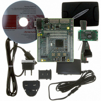
Manufacturer Part Number
R0K561622S000BE
Description
KIT STARTER FOR H8SX/1622
Manufacturer
Renesas Electronics America
Series
Renesas Starter Kits (RSK)r
Type
MCUr
Specifications of R0K561622S000BE
Contents
Board, Cables, CD, Debugger, Power Supply
Silicon Manufacturer
Renesas
Features
Coding And Debugging, E10A Emulator, RS232 Serial Connection
Kit Contents
Board
Silicon Family Name
H8SX/1622F
Silicon Core Number
R5F61622N50LGV
Lead Free Status / RoHS Status
Lead free / RoHS Compliant
For Use With/related Products
H8SX/1622
Lead Free Status / RoHS Status
Lead free / RoHS Compliant, Lead free / RoHS Compliant


Section 22 Flash Memory
22.8.4
In the descriptions in this manual, the on-chip programs and program data storage areas are
assumed to be in the on-chip RAM. However, they can be executed from part of the flash memory
which is not to be programmed or erased as long as the following conditions are satisfied.
• The on-chip program is downloaded to and executed in the on-chip RAM specified by
• Since the on-chip program uses a stack area, allocate 128 bytes at the maximum as a stack
• Download requested by setting the SCO bit in FCCS to 1 should be executed from the on-chip
• In an operating mode in which the external address space is not accessible, such as single-chip
• The flash memory is not accessible during programming/erasure. Programming/erasure is
• After programming/erasure starts, access to the flash memory should be inhibited until FKEY
• Switching of the memory MATs by FMATS should be needed when programming/erasure of
• When the program data storage area is within the flash memory area, an error will occur even
Rev. 2.00 Sep. 16, 2009 Page 824 of 1036
REJ09B0414-0200
FTDAR. Therefore, this on-chip RAM area is not available for use.
area.
RAM because it will require switching of the memory MATs.
mode, the required procedure programs, NMI handling vector table, and NMI handling routine
should be transferred to the on-chip RAM before programming/erasure starts (download result
is determined).
executed by the program downloaded to the on-chip RAM. Therefore, the procedure program
that initiates operation, the NMI handling vector table, and the NMI handling routine should be
stored in the on-chip RAM other than the flash memory.
is cleared. The reset input state (period of RES = 0) must be set to at least 100 µs when the
operating mode is changed and the reset start executed on completion of programming/erasure.
Transitions to the reset state are inhibited during programming/erasure. When the reset signal
is input, a reset input state (period of RES = 0) of at least 100 µs is needed before the reset
signal is released.
the user MAT is operated in user boot mode. The program which switches the memory MATs
should be executed from the on-chip RAM. For details, see section 22.11, Switching between
User MAT and User Boot MAT. Make sure you know which memory MAT is currently
selected when switching them.
when the data stored is normal program data. Therefore, the data should be transferred to the
on-chip RAM to place the address that the FMPDR parameter indicates in an area other than
the flash memory.
On-Chip Program and Storable Area for Program Data
Related parts for R0K561622S000BE
Image
Part Number
Description
Manufacturer
Datasheet
Request
R

Part Number:
Description:
KIT STARTER FOR M16C/29
Manufacturer:
Renesas Electronics America
Datasheet:

Part Number:
Description:
KIT STARTER FOR R8C/2D
Manufacturer:
Renesas Electronics America
Datasheet:

Part Number:
Description:
R0K33062P STARTER KIT
Manufacturer:
Renesas Electronics America
Datasheet:

Part Number:
Description:
KIT STARTER FOR R8C/23 E8A
Manufacturer:
Renesas Electronics America
Datasheet:

Part Number:
Description:
KIT STARTER FOR R8C/25
Manufacturer:
Renesas Electronics America
Datasheet:

Part Number:
Description:
KIT STARTER H8S2456 SHARPE DSPLY
Manufacturer:
Renesas Electronics America
Datasheet:

Part Number:
Description:
KIT STARTER FOR R8C38C
Manufacturer:
Renesas Electronics America
Datasheet:

Part Number:
Description:
KIT STARTER FOR R8C35C
Manufacturer:
Renesas Electronics America
Datasheet:

Part Number:
Description:
KIT STARTER FOR R8CL3AC+LCD APPS
Manufacturer:
Renesas Electronics America
Datasheet:
Part Number:
Description:
KIT STARTER FOR RX610
Manufacturer:
Renesas Electronics America
Datasheet:

Part Number:
Description:
KIT STARTER FOR R32C/118
Manufacturer:
Renesas Electronics America
Datasheet:

Part Number:
Description:
KIT DEV RSK-R8C/26-29
Manufacturer:
Renesas Electronics America
Datasheet:

Part Number:
Description:
KIT STARTER FOR SH7124
Manufacturer:
Renesas Electronics America
Datasheet:

Part Number:
Description:
KIT DEV FOR SH7203
Manufacturer:
Renesas Electronics America
Datasheet:
Part Number:
Description:
KIT STARTER FOR R8C/18191A1B
Manufacturer:
Renesas Electronics America
Datasheet: