R0K561622S000BE Renesas Electronics America, R0K561622S000BE Datasheet - Page 696
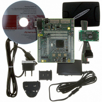
R0K561622S000BE
Manufacturer Part Number
R0K561622S000BE
Description
KIT STARTER FOR H8SX/1622
Manufacturer
Renesas Electronics America
Series
Renesas Starter Kits (RSK)r
Type
MCUr
Specifications of R0K561622S000BE
Contents
Board, Cables, CD, Debugger, Power Supply
Silicon Manufacturer
Renesas
Features
Coding And Debugging, E10A Emulator, RS232 Serial Connection
Kit Contents
Board
Silicon Family Name
H8SX/1622F
Silicon Core Number
R5F61622N50LGV
Lead Free Status / RoHS Status
Lead free / RoHS Compliant
For Use With/related Products
H8SX/1622
Lead Free Status / RoHS Status
Lead free / RoHS Compliant, Lead free / RoHS Compliant


Section 16 Serial Communication Interface (SCI)
16.7.5
Before transmitting and receiving data, initialize the SCI using the following procedure.
Initialization is also necessary before switching from transmission to reception and vice versa.
1. Clear the TE and RE bits in SCR to 0.
2. Set the ICR bit of the corresponding pin to 1.
3. Clear the error flags ERS, PER, and ORER in SSR to 0.
4. Set the GM, BLK, O/E, BCP1, BCP0, CKS1, and CKS0 bits in SMR appropriately. Also set
5. Set the SMIF, SDIR, and SINV bits in SCMR appropriately. When the DDR corresponding to
6. Set the value corresponding to the bit rate in BRR.
7. Set the CKE1 and CKE0 bits in SCR appropriately. Clear the TIE, RIE, TE, RE, MPIE, and
8. Set the TIE, RIE, TE, and RE bits in SCR appropriately after waiting for at least a 1-bit
To switch from reception to transmission, first verify that reception has completed, then initialize
the SCI. At the end of initialization, RE and TE should be set to 0 and 1, respectively. Reception
completion can be verified by reading the RDRF, PER, or ORER flag. To switch from
transmission to reception, first verify that transmission has completed, then initialize the SCI. At
the end of initialization, TE and RE should be set to 0 and 1, respectively. Transmission
completion can be verified by reading the TEND flag.
Rev. 2.00 Sep. 16, 2009 Page 666 of 1036
REJ09B0414-0200
the PE bit to 1.
the TxD pin is cleared to 0, the TxD and RxD pins are changed from port pins to SCI pins,
placing the pins into high impedance state.
TEIE bits to 0 simultaneously.
When the CKE0 bit is set to 1, the SCK pin is allowed to output clock pulses.
interval. Setting the TE and RE bits to 1 simultaneously is prohibited except for self diagnosis.
Initialization
Related parts for R0K561622S000BE
Image
Part Number
Description
Manufacturer
Datasheet
Request
R

Part Number:
Description:
KIT STARTER FOR M16C/29
Manufacturer:
Renesas Electronics America
Datasheet:

Part Number:
Description:
KIT STARTER FOR R8C/2D
Manufacturer:
Renesas Electronics America
Datasheet:

Part Number:
Description:
R0K33062P STARTER KIT
Manufacturer:
Renesas Electronics America
Datasheet:

Part Number:
Description:
KIT STARTER FOR R8C/23 E8A
Manufacturer:
Renesas Electronics America
Datasheet:

Part Number:
Description:
KIT STARTER FOR R8C/25
Manufacturer:
Renesas Electronics America
Datasheet:

Part Number:
Description:
KIT STARTER H8S2456 SHARPE DSPLY
Manufacturer:
Renesas Electronics America
Datasheet:

Part Number:
Description:
KIT STARTER FOR R8C38C
Manufacturer:
Renesas Electronics America
Datasheet:

Part Number:
Description:
KIT STARTER FOR R8C35C
Manufacturer:
Renesas Electronics America
Datasheet:

Part Number:
Description:
KIT STARTER FOR R8CL3AC+LCD APPS
Manufacturer:
Renesas Electronics America
Datasheet:
Part Number:
Description:
KIT STARTER FOR RX610
Manufacturer:
Renesas Electronics America
Datasheet:

Part Number:
Description:
KIT STARTER FOR R32C/118
Manufacturer:
Renesas Electronics America
Datasheet:

Part Number:
Description:
KIT DEV RSK-R8C/26-29
Manufacturer:
Renesas Electronics America
Datasheet:

Part Number:
Description:
KIT STARTER FOR SH7124
Manufacturer:
Renesas Electronics America
Datasheet:

Part Number:
Description:
KIT DEV FOR SH7203
Manufacturer:
Renesas Electronics America
Datasheet:
Part Number:
Description:
KIT STARTER FOR R8C/18191A1B
Manufacturer:
Renesas Electronics America
Datasheet: