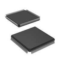
HD6417751RF240V Renesas Electronics America, HD6417751RF240V Datasheet - Page 85

HD6417751RF240V
Manufacturer Part Number
HD6417751RF240V
Description
MPU 1.5/3.3V 0K PB-FREE 256-QFP
Manufacturer
Renesas Electronics America
Series
SuperH® SH7750r
Datasheet
1.D6417751RBP200DV.pdf
(1226 pages)
Specifications of HD6417751RF240V
Core Processor
SH-4
Core Size
32-Bit
Speed
240MHz
Connectivity
EBI/EMI, FIFO, SCI, SmartCard
Peripherals
DMA, POR, WDT
Number Of I /o
39
Program Memory Type
ROMless
Ram Size
48K x 8
Voltage - Supply (vcc/vdd)
1.4 V ~ 1.6 V
Oscillator Type
External
Operating Temperature
-20°C ~ 75°C
Package / Case
256-QFP Exposed Pad, 256-eQFP, 256-HQFP
Lead Free Status / RoHS Status
Lead free / RoHS Compliant
Eeprom Size
-
Program Memory Size
-
Data Converters
-
Available stocks
Company
Part Number
Manufacturer
Quantity
Price
Company:
Part Number:
HD6417751RF240V
Manufacturer:
Renesas Electronics America
Quantity:
10 000
- Current page: 85 of 1226
- Download datasheet (7Mb)
Figure 15.20 Sample Serial Transmission Flowchart .................................................................. 658
Figure 15.21 Example of SCI Transmit Operation ...................................................................... 660
Figure 15.22 Sample Serial Reception Flowchart (1).................................................................. 661
Figure 15.23 Example of SCI Receive Operation........................................................................ 663
Figure 15.24 Sample Flowchart for Serial Data Transmission and Reception ............................ 664
Figure 15.25 Receive Data Sampling Timing in Asynchronous Mode ....................................... 668
Figure 15.26 Example of Synchronous Transmission by DMAC ............................................... 669
Section 16 Serial Communication Interface with FIFO (SCIF)
Figure 16.1 Block Diagram of SCIF.......................................................................................... 673
Figure 16.2 MD8/RTS2 Pin....................................................................................................... 696
Figure 16.3 MD7/CTS2 Pin....................................................................................................... 697
Figure 16.4 MD1/TxD2 Pin....................................................................................................... 698
Figure 16.5 MD2/RxD2 Pin ...................................................................................................... 698
Figure 16.6 MD0/SCK2 Pin ...................................................................................................... 699
Figure 16.7 Sample SCIF Initialization Flowchart .................................................................... 705
Figure 16.8 Sample Serial Transmission Flowchart .................................................................. 706
Figure 16.9 Example of Transmit Operation (Example with 8-Bit Data, Parity,
Figure 16.10 Example of Operation Using Modem Control (CTS2)........................................... 708
Figure 16.11 Sample Serial Reception Flowchart (1).................................................................. 709
Figure 16.11 Sample Serial Reception Flowchart (2).................................................................. 710
Figure 16.12 Example of SCIF Receive Operation (Example with 8-Bit Data, Parity,
Figure 16.13 Example of Operation Using Modem Control (RTS2)........................................... 712
Figure 16.14 Receive Data Sampling Timing in Asynchronous Mode ....................................... 716
Section 17 Smart Card Interface
Figure 17.1 Block Diagram of Smart Card Interface................................................................. 720
Figure 17.2 Schematic Diagram of Smart Card Interface Pin Connections............................... 727
Figure 17.3 Smart Card Interface Data Format ......................................................................... 728
Figure 17.4 TEND Generation Timing...................................................................................... 730
Figure 17.5 Sample Start Character Waveforms ....................................................................... 731
Figure 17.6 Difference in Clock Output According to GM Bit Setting..................................... 734
Figure 17.7 Sample Initialization Flowchart ............................................................................. 735
Figure 17.8 Sample Transmission Processing Flowchart .......................................................... 737
Figure 17.9 Sample Reception Processing Flowchart ............................................................... 739
Figure 17.10 Receive Data Sampling Timing in Smart Card Mode ............................................ 741
Figure 17.11 Retransfer Operation in SCI Receive Mode ........................................................... 743
Figure 17.12 Retransfer Operation in SCI Transmit Mode.......................................................... 743
One Stop Bit).......................................................................................................... 708
One Stop Bit).......................................................................................................... 712
Rev.4.00 Oct. 10, 2008 Page lxxxiii of xcviii
REJ09B0370-0400
Related parts for HD6417751RF240V
Image
Part Number
Description
Manufacturer
Datasheet
Request
R

Part Number:
Description:
KIT STARTER FOR M16C/29
Manufacturer:
Renesas Electronics America
Datasheet:

Part Number:
Description:
KIT STARTER FOR R8C/2D
Manufacturer:
Renesas Electronics America
Datasheet:

Part Number:
Description:
R0K33062P STARTER KIT
Manufacturer:
Renesas Electronics America
Datasheet:

Part Number:
Description:
KIT STARTER FOR R8C/23 E8A
Manufacturer:
Renesas Electronics America
Datasheet:

Part Number:
Description:
KIT STARTER FOR R8C/25
Manufacturer:
Renesas Electronics America
Datasheet:

Part Number:
Description:
KIT STARTER H8S2456 SHARPE DSPLY
Manufacturer:
Renesas Electronics America
Datasheet:

Part Number:
Description:
KIT STARTER FOR R8C38C
Manufacturer:
Renesas Electronics America
Datasheet:

Part Number:
Description:
KIT STARTER FOR R8C35C
Manufacturer:
Renesas Electronics America
Datasheet:

Part Number:
Description:
KIT STARTER FOR R8CL3AC+LCD APPS
Manufacturer:
Renesas Electronics America
Datasheet:

Part Number:
Description:
KIT STARTER FOR RX610
Manufacturer:
Renesas Electronics America
Datasheet:

Part Number:
Description:
KIT STARTER FOR R32C/118
Manufacturer:
Renesas Electronics America
Datasheet:

Part Number:
Description:
KIT DEV RSK-R8C/26-29
Manufacturer:
Renesas Electronics America
Datasheet:

Part Number:
Description:
KIT STARTER FOR SH7124
Manufacturer:
Renesas Electronics America
Datasheet:

Part Number:
Description:
KIT STARTER FOR H8SX/1622
Manufacturer:
Renesas Electronics America
Datasheet:

Part Number:
Description:
KIT DEV FOR SH7203
Manufacturer:
Renesas Electronics America
Datasheet:


