HD6417751RF240V Renesas Electronics America, HD6417751RF240V Datasheet - Page 64
HD6417751RF240V
Manufacturer Part Number
HD6417751RF240V
Description
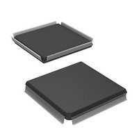
MPU 1.5/3.3V 0K PB-FREE 256-QFP
Manufacturer
Renesas Electronics America
Series
SuperH® SH7750r
Datasheet
1.D6417751RBP200DV.pdf
(1226 pages)
Specifications of HD6417751RF240V
Core Processor
SH-4
Core Size
32-Bit
Speed
240MHz
Connectivity
EBI/EMI, FIFO, SCI, SmartCard
Peripherals
DMA, POR, WDT
Number Of I /o
39
Program Memory Type
ROMless
Ram Size
48K x 8
Voltage - Supply (vcc/vdd)
1.4 V ~ 1.6 V
Oscillator Type
External
Operating Temperature
-20°C ~ 75°C
Package / Case
256-QFP Exposed Pad, 256-eQFP, 256-HQFP
Lead Free Status / RoHS Status
Lead free / RoHS Compliant
Eeprom Size
-
Program Memory Size
-
Data Converters
-
Available stocks
Company
Part Number
Manufacturer
Quantity
Price
Company:

Part Number:
HD6417751RF240V
Manufacturer:
Renesas Electronics America
Quantity:
10 000


9.10 Usage Notes ...................................................................................................................... 264
Section 10 Clock Oscillation Circuits
10.1 Overview........................................................................................................................... 267
10.2 Overview of CPG.............................................................................................................. 269
10.3 Clock Operating Modes .................................................................................................... 273
10.4 CPG Register Description................................................................................................. 275
10.5 Changing the Frequency ................................................................................................... 278
10.6 Output Clock Control........................................................................................................ 280
10.7 Overview of Watchdog Timer .......................................................................................... 280
10.8 WDT Register Descriptions .............................................................................................. 281
10.9 Using the WDT ................................................................................................................. 285
10.10 Notes on Board Design ..................................................................................................... 287
10.11 Usage Notes ...................................................................................................................... 289
Rev.4.00 Oct. 10, 2008 Page lxii of xcviii
REJ09B0370-0400
9.9.1
9.9.2
9.9.3
9.9.4
9.9.5
9.10.1 Note on Current Consumption ............................................................................. 264
10.1.1 Features................................................................................................................ 267
10.2.1 Block Diagram of CPG........................................................................................ 269
10.2.2 CPG Pin Configuration ........................................................................................ 272
10.2.3 CPG Register Configuration ................................................................................ 272
10.4.1 Frequency Control Register (FRQCR)................................................................. 275
10.5.1 Changing PLL Circuit 1 Starting/Stopping (When PLL Circuit 2 Is Off) ........... 278
10.5.2 Changing PLL Circuit 1 Starting/Stopping (When PLL Circuit 2 Is On)............ 278
10.5.3 Changing Bus Clock Division Ratio (When PLL Circuit 2 Is On) ...................... 279
10.5.4 Changing Bus Clock Division Ratio (When PLL Circuit 2 Is Off) ..................... 279
10.5.5 Changing CPU or Peripheral Module Clock Division Ratio ............................... 279
10.7.1 Block Diagram..................................................................................................... 280
10.7.2 Register Configuration......................................................................................... 281
10.8.1 Watchdog Timer Counter (WTCNT)................................................................... 281
10.8.2 Watchdog Timer Control/Status Register (WTCSR)........................................... 282
10.8.3 Notes on Register Access..................................................................................... 284
10.9.1 Standby Clearing Procedure ................................................................................ 285
10.9.2 Frequency Changing Procedure ........................................................................... 285
10.9.3 Using Watchdog Timer Mode.............................................................................. 286
10.9.4 Using Interval Timer Mode ................................................................................. 286
10.11.1 Invalid Manual Reset Triggered by Watchdog Timer (SH7751 Only)................ 289
In Reset ................................................................................................................ 255
In Exit from Standby Mode ................................................................................. 256
In Exit from Sleep Mode...................................................................................... 257
In Exit from Deep Sleep Mode ............................................................................ 260
Hardware Standby Mode Timing......................................................................... 262
........................................................................... 267
Related parts for HD6417751RF240V
Image
Part Number
Description
Manufacturer
Datasheet
Request
R

Part Number:
Description:
KIT STARTER FOR M16C/29
Manufacturer:
Renesas Electronics America
Datasheet:

Part Number:
Description:
KIT STARTER FOR R8C/2D
Manufacturer:
Renesas Electronics America
Datasheet:

Part Number:
Description:
R0K33062P STARTER KIT
Manufacturer:
Renesas Electronics America
Datasheet:

Part Number:
Description:
KIT STARTER FOR R8C/23 E8A
Manufacturer:
Renesas Electronics America
Datasheet:

Part Number:
Description:
KIT STARTER FOR R8C/25
Manufacturer:
Renesas Electronics America
Datasheet:

Part Number:
Description:
KIT STARTER H8S2456 SHARPE DSPLY
Manufacturer:
Renesas Electronics America
Datasheet:

Part Number:
Description:
KIT STARTER FOR R8C38C
Manufacturer:
Renesas Electronics America
Datasheet:

Part Number:
Description:
KIT STARTER FOR R8C35C
Manufacturer:
Renesas Electronics America
Datasheet:

Part Number:
Description:
KIT STARTER FOR R8CL3AC+LCD APPS
Manufacturer:
Renesas Electronics America
Datasheet:
Part Number:
Description:
KIT STARTER FOR RX610
Manufacturer:
Renesas Electronics America
Datasheet:

Part Number:
Description:
KIT STARTER FOR R32C/118
Manufacturer:
Renesas Electronics America
Datasheet:

Part Number:
Description:
KIT DEV RSK-R8C/26-29
Manufacturer:
Renesas Electronics America
Datasheet:

Part Number:
Description:
KIT STARTER FOR SH7124
Manufacturer:
Renesas Electronics America
Datasheet:

Part Number:
Description:
KIT STARTER FOR H8SX/1622
Manufacturer:
Renesas Electronics America
Datasheet:

Part Number:
Description:
KIT DEV FOR SH7203
Manufacturer:
Renesas Electronics America
Datasheet: