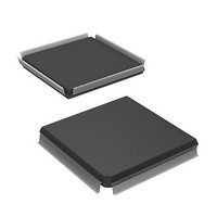
HD6417751RF240V Renesas Electronics America, HD6417751RF240V Datasheet - Page 533

HD6417751RF240V
Manufacturer Part Number
HD6417751RF240V
Description
MPU 1.5/3.3V 0K PB-FREE 256-QFP
Manufacturer
Renesas Electronics America
Series
SuperH® SH7750r
Datasheet
1.D6417751RBP200DV.pdf
(1226 pages)
Specifications of HD6417751RF240V
Core Processor
SH-4
Core Size
32-Bit
Speed
240MHz
Connectivity
EBI/EMI, FIFO, SCI, SmartCard
Peripherals
DMA, POR, WDT
Number Of I /o
39
Program Memory Type
ROMless
Ram Size
48K x 8
Voltage - Supply (vcc/vdd)
1.4 V ~ 1.6 V
Oscillator Type
External
Operating Temperature
-20°C ~ 75°C
Package / Case
256-QFP Exposed Pad, 256-eQFP, 256-HQFP
Lead Free Status / RoHS Status
Lead free / RoHS Compliant
Eeprom Size
-
Program Memory Size
-
Data Converters
-
Available stocks
Company
Part Number
Manufacturer
Quantity
Price
Company:
Part Number:
HD6417751RF240V
Manufacturer:
Renesas Electronics America
Quantity:
10 000
- Current page: 533 of 1226
- Download datasheet (7Mb)
Burst Write: The timing chart for a burst write is shown in figure 13.26. In this LSI, a burst write
occurs only in the event of 32-byte transfer. In a burst write operation, the WRIT command is
issued in the Tc1 cycle following the Tr cycle in which the ACTV command is output and, 4
cycles later, the WRITA command is issued. In the write cycle, the write data is output at the same
time as the write command. In the case of the write with auto-precharge command, precharging of
the relevant bank is performed in the synchronous DRAM after completion of the write command,
and therefore no command can be issued for the same bank until precharging is completed.
Consequently, in addition to the precharge wait cycle, Tpc, used in a read access, cycle Trwl is
also added as a wait interval until precharging is started following the write command. Issuance of
a new command for the synchronous DRAM is postponed during this interval. The number of
Trwl cycles can be specified by bits TRWL2–TRWL0 in MCR. Access starts from 16-byte
Note: For DACKn, an example is shown where CHCRn.AL (access level) = 0 for the DMAC.
CKIO
Bank
Precharge-sel
Address
CSn
RD/WR
RAS
CASS
DQMn
D31–D0
(read)
BS
CKE
DACKn
(SA: IO ← memory)
Figure 13.25 Basic Timing for Synchronous DRAM Single Read
Tr
Row
Row
Row
Trw
Tc1
Tc2
Tc3 Tc4/Td1 Td2
Rev.4.00 Oct. 10, 2008 Page 433 of 1122
H/L
c1
c1
13. Bus State Controller (BSC)
Td3
Td4
Tpc
REJ09B0370-0400
Related parts for HD6417751RF240V
Image
Part Number
Description
Manufacturer
Datasheet
Request
R

Part Number:
Description:
KIT STARTER FOR M16C/29
Manufacturer:
Renesas Electronics America
Datasheet:

Part Number:
Description:
KIT STARTER FOR R8C/2D
Manufacturer:
Renesas Electronics America
Datasheet:

Part Number:
Description:
R0K33062P STARTER KIT
Manufacturer:
Renesas Electronics America
Datasheet:

Part Number:
Description:
KIT STARTER FOR R8C/23 E8A
Manufacturer:
Renesas Electronics America
Datasheet:

Part Number:
Description:
KIT STARTER FOR R8C/25
Manufacturer:
Renesas Electronics America
Datasheet:

Part Number:
Description:
KIT STARTER H8S2456 SHARPE DSPLY
Manufacturer:
Renesas Electronics America
Datasheet:

Part Number:
Description:
KIT STARTER FOR R8C38C
Manufacturer:
Renesas Electronics America
Datasheet:

Part Number:
Description:
KIT STARTER FOR R8C35C
Manufacturer:
Renesas Electronics America
Datasheet:

Part Number:
Description:
KIT STARTER FOR R8CL3AC+LCD APPS
Manufacturer:
Renesas Electronics America
Datasheet:

Part Number:
Description:
KIT STARTER FOR RX610
Manufacturer:
Renesas Electronics America
Datasheet:

Part Number:
Description:
KIT STARTER FOR R32C/118
Manufacturer:
Renesas Electronics America
Datasheet:

Part Number:
Description:
KIT DEV RSK-R8C/26-29
Manufacturer:
Renesas Electronics America
Datasheet:

Part Number:
Description:
KIT STARTER FOR SH7124
Manufacturer:
Renesas Electronics America
Datasheet:

Part Number:
Description:
KIT STARTER FOR H8SX/1622
Manufacturer:
Renesas Electronics America
Datasheet:

Part Number:
Description:
KIT DEV FOR SH7203
Manufacturer:
Renesas Electronics America
Datasheet:


