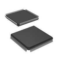
HD6417751RF240V Renesas Electronics America, HD6417751RF240V Datasheet - Page 172

HD6417751RF240V
Manufacturer Part Number
HD6417751RF240V
Description
MPU 1.5/3.3V 0K PB-FREE 256-QFP
Manufacturer
Renesas Electronics America
Series
SuperH® SH7750r
Datasheet
1.D6417751RBP200DV.pdf
(1226 pages)
Specifications of HD6417751RF240V
Core Processor
SH-4
Core Size
32-Bit
Speed
240MHz
Connectivity
EBI/EMI, FIFO, SCI, SmartCard
Peripherals
DMA, POR, WDT
Number Of I /o
39
Program Memory Type
ROMless
Ram Size
48K x 8
Voltage - Supply (vcc/vdd)
1.4 V ~ 1.6 V
Oscillator Type
External
Operating Temperature
-20°C ~ 75°C
Package / Case
256-QFP Exposed Pad, 256-eQFP, 256-HQFP
Lead Free Status / RoHS Status
Lead free / RoHS Compliant
Eeprom Size
-
Program Memory Size
-
Data Converters
-
Available stocks
Company
Part Number
Manufacturer
Quantity
Price
Company:
Part Number:
HD6417751RF240V
Manufacturer:
Renesas Electronics America
Quantity:
10 000
- Current page: 172 of 1226
- Download datasheet (7Mb)
3. Memory Management Unit (MMU)
CHCRn.DSAn, CHCRn.STC, and CHCRn.DTC values. For details, see section 14, Direct
Memory Access Controller (DMAC).
P0, P1, P3, U0 Areas: The P0, P1, P3, and U0 areas can be accessed using the cache. Whether or
not the cache is used is determined by the cache control register (CCR). When the cache is used,
with the exception of the P1 area, switching between the copy-back method and the write-through
method for write accesses is specified by the CCR.WT bit. For the P1 area, switching is specified
by the CCR.CB bit. Zeroizing the upper 3 bits of an address in these areas gives the corresponding
external memory space address. However, since area 7 in the external memory space is a reserved
area, a reserved area also appears in these areas.
P2 Area: The P2 area cannot be accessed using the cache. In the P2 area, zeroizing the upper 3
bits of an address gives the corresponding external memory space address. However, since area 7
in the external memory space is a reserved area, a reserved area also appears in this area.
P4 Area: The P4 area is mapped onto SH-4 on-chip I/O channels. This area cannot be accessed
using the cache. The P4 area is shown in detail in figure 3.4.
Rev.4.00 Oct. 10, 2008 Page 72 of 1122
REJ09B0370-0400
H'E000 0000
H'E400 0000
H'F000 0000
H'F100 0000
H'F200 0000
H'F300 0000
H'F400 0000
H'F500 0000
H'F600 0000
H'F700 0000
H'F800 0000
H'FC00 0000
H'FFFF FFFF
Figure 3.4 P4 Area
Instruction TLB data arrays 1 and 2
Unified TLB data arrays 1 and 2
Instruction cache address array
Operand cache address array
Instruction TLB address array
Instruction cache data array
Operand cache data array
Unified TLB address array
Control register area
Reserved area
Reserved area
Store queue
Related parts for HD6417751RF240V
Image
Part Number
Description
Manufacturer
Datasheet
Request
R

Part Number:
Description:
KIT STARTER FOR M16C/29
Manufacturer:
Renesas Electronics America
Datasheet:

Part Number:
Description:
KIT STARTER FOR R8C/2D
Manufacturer:
Renesas Electronics America
Datasheet:

Part Number:
Description:
R0K33062P STARTER KIT
Manufacturer:
Renesas Electronics America
Datasheet:

Part Number:
Description:
KIT STARTER FOR R8C/23 E8A
Manufacturer:
Renesas Electronics America
Datasheet:

Part Number:
Description:
KIT STARTER FOR R8C/25
Manufacturer:
Renesas Electronics America
Datasheet:

Part Number:
Description:
KIT STARTER H8S2456 SHARPE DSPLY
Manufacturer:
Renesas Electronics America
Datasheet:

Part Number:
Description:
KIT STARTER FOR R8C38C
Manufacturer:
Renesas Electronics America
Datasheet:

Part Number:
Description:
KIT STARTER FOR R8C35C
Manufacturer:
Renesas Electronics America
Datasheet:

Part Number:
Description:
KIT STARTER FOR R8CL3AC+LCD APPS
Manufacturer:
Renesas Electronics America
Datasheet:

Part Number:
Description:
KIT STARTER FOR RX610
Manufacturer:
Renesas Electronics America
Datasheet:

Part Number:
Description:
KIT STARTER FOR R32C/118
Manufacturer:
Renesas Electronics America
Datasheet:

Part Number:
Description:
KIT DEV RSK-R8C/26-29
Manufacturer:
Renesas Electronics America
Datasheet:

Part Number:
Description:
KIT STARTER FOR SH7124
Manufacturer:
Renesas Electronics America
Datasheet:

Part Number:
Description:
KIT STARTER FOR H8SX/1622
Manufacturer:
Renesas Electronics America
Datasheet:

Part Number:
Description:
KIT DEV FOR SH7203
Manufacturer:
Renesas Electronics America
Datasheet:


