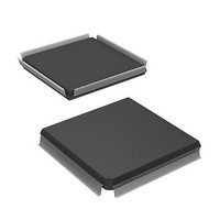
HD6417751RF240V Renesas Electronics America, HD6417751RF240V Datasheet - Page 1052

HD6417751RF240V
Manufacturer Part Number
HD6417751RF240V
Description
MPU 1.5/3.3V 0K PB-FREE 256-QFP
Manufacturer
Renesas Electronics America
Series
SuperH® SH7750r
Datasheet
1.D6417751RBP200DV.pdf
(1226 pages)
Specifications of HD6417751RF240V
Core Processor
SH-4
Core Size
32-Bit
Speed
240MHz
Connectivity
EBI/EMI, FIFO, SCI, SmartCard
Peripherals
DMA, POR, WDT
Number Of I /o
39
Program Memory Type
ROMless
Ram Size
48K x 8
Voltage - Supply (vcc/vdd)
1.4 V ~ 1.6 V
Oscillator Type
External
Operating Temperature
-20°C ~ 75°C
Package / Case
256-QFP Exposed Pad, 256-eQFP, 256-HQFP
Lead Free Status / RoHS Status
Lead free / RoHS Compliant
Eeprom Size
-
Program Memory Size
-
Data Converters
-
Available stocks
Company
Part Number
Manufacturer
Quantity
Price
Company:
Part Number:
HD6417751RF240V
Manufacturer:
Renesas Electronics America
Quantity:
10 000
- Current page: 1052 of 1226
- Download datasheet (7Mb)
22. PCI Controller (PCIC)
Target Read/Write Cycle Timing: The PCIC responds to target memory read accesses from an
external master by retries until 8 longword data are prepared in the PCIC's internal FIFO. That is,
it always responds to the first target read with a retry.
Also, if a target memory write access is made, the PCIC responds to all subsequent target memory
accesses with a retry until the write data is completely written to local memory. Thus, the content
of the data is guaranteed when data written to the target is immediately subject to a target read
operation.
The following restrictions apply to the SH7751. With the SH7751R, in the following case the
values of data are discarded for a target read that is executed immediately after a target write
because the data read in an earlier read operation that was carried out by a different PCI device are
discarded.
[Restrictions]
In a system in which access is made to the same address*
devices, the data cannot be guaranteed when a target read is performed immediately after a target
write.
The possibility of an error occurs when the target read immediately after the target write gets bus
privileges at the point the data is ready for a target read by a different PCI device prior to the target
write. In this case, the data prior to the target write is read. If such transfers are likely to occur,
implement either (a) or (b) below.
(a) If using the data that has been read, perform two read operations and use only the data from the
(b) If not using the data that has been read (if you are performing the read operation in order to
Notes: 1. Address matching AD[31:2] in the address phase.
Only single transfers are supported in the case of target accesses of the configuration space and
I/O space. If there is a burst access request, the external master is disconnected on completion of
the first transfer.
Note that the DEVSEL response speed is fixed at 2 clocks (Medium) in the case of target access of
the PCIC.
Rev.4.00 Oct. 10, 2008 Page 952 of 1122
REJ09B0370-0400
second read operation.
determine the timing for actually writing data to the destination), be sure that the read
address*
2. The address that does not correspond to the address AD[31:2] on a longword boundary.
2
immediately after writing is different from the write address.
1
in local memory by two or more PCI
Related parts for HD6417751RF240V
Image
Part Number
Description
Manufacturer
Datasheet
Request
R

Part Number:
Description:
KIT STARTER FOR M16C/29
Manufacturer:
Renesas Electronics America
Datasheet:

Part Number:
Description:
KIT STARTER FOR R8C/2D
Manufacturer:
Renesas Electronics America
Datasheet:

Part Number:
Description:
R0K33062P STARTER KIT
Manufacturer:
Renesas Electronics America
Datasheet:

Part Number:
Description:
KIT STARTER FOR R8C/23 E8A
Manufacturer:
Renesas Electronics America
Datasheet:

Part Number:
Description:
KIT STARTER FOR R8C/25
Manufacturer:
Renesas Electronics America
Datasheet:

Part Number:
Description:
KIT STARTER H8S2456 SHARPE DSPLY
Manufacturer:
Renesas Electronics America
Datasheet:

Part Number:
Description:
KIT STARTER FOR R8C38C
Manufacturer:
Renesas Electronics America
Datasheet:

Part Number:
Description:
KIT STARTER FOR R8C35C
Manufacturer:
Renesas Electronics America
Datasheet:

Part Number:
Description:
KIT STARTER FOR R8CL3AC+LCD APPS
Manufacturer:
Renesas Electronics America
Datasheet:

Part Number:
Description:
KIT STARTER FOR RX610
Manufacturer:
Renesas Electronics America
Datasheet:

Part Number:
Description:
KIT STARTER FOR R32C/118
Manufacturer:
Renesas Electronics America
Datasheet:

Part Number:
Description:
KIT DEV RSK-R8C/26-29
Manufacturer:
Renesas Electronics America
Datasheet:

Part Number:
Description:
KIT STARTER FOR SH7124
Manufacturer:
Renesas Electronics America
Datasheet:

Part Number:
Description:
KIT STARTER FOR H8SX/1622
Manufacturer:
Renesas Electronics America
Datasheet:

Part Number:
Description:
KIT DEV FOR SH7203
Manufacturer:
Renesas Electronics America
Datasheet:


