DF2328BVF25V Renesas Electronics America, DF2328BVF25V Datasheet - Page 964
DF2328BVF25V
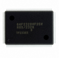
Manufacturer Part Number
DF2328BVF25V
Description
IC H8S MCU FLASH 256K 128QFP
Manufacturer
Renesas Electronics America
Series
H8® H8S/2300r
Datasheets
1.HEWH8E10A.pdf
(19 pages)
2.D12312SVTE25V.pdf
(341 pages)
3.D12322RVF25V.pdf
(1304 pages)
Specifications of DF2328BVF25V
Core Processor
H8S/2000
Core Size
16-Bit
Speed
25MHz
Connectivity
SCI, SmartCard
Peripherals
DMA, POR, PWM, WDT
Number Of I /o
87
Program Memory Size
256KB (256K x 8)
Program Memory Type
FLASH
Ram Size
8K x 8
Voltage - Supply (vcc/vdd)
2.7 V ~ 3.6 V
Data Converters
A/D 8x10b; D/A 2x8b
Oscillator Type
Internal
Operating Temperature
-20°C ~ 75°C
Package / Case
128-QFP
For Use With
EDK2329 - DEV EVALUATION KIT H8S/2329
Lead Free Status / RoHS Status
Lead free / RoHS Compliant
Eeprom Size
-
Other names
HD64F2328BVF25V
Available stocks
Company
Part Number
Manufacturer
Quantity
Price
Company:

Part Number:
DF2328BVF25V
Manufacturer:
Renesas Electronics America
Quantity:
10 000


Section 21 Power-Down Modes
21.7
21.7.1
When the STBY pin is driven low, a transition is made to hardware standby mode from any mode.
In hardware standby mode, all functions enter the reset state and stop operation, resulting in a
significant reduction in power dissipation. As long as the prescribed voltage is supplied, on-chip
RAM data is retained. I/O ports are set to the high-impedance state.
In order to retain on-chip RAM data, the RAME bit in SYSCR should be cleared to 0 before
driving the STBY pin low.
Do not change the state of the mode pins (MD2 to MD0) while the chip is in hardware standby
mode.
Hardware standby mode is cleared by means of the STBY pin and the RES pin. When the STBY
pin is driven high while the RES pin is low, the reset state is set and clock oscillation is started.
Ensure that the RES pin is held low until the clock oscillator stabilizes (at least 8 ms—the
oscillation stabilization time—when using a crystal oscillator). When the RES pin is subsequently
driven high, a transition is made to the program execution state via the reset exception handling
state.
21.7.2
Figure 21.3 shows an example of hardware standby mode timing.
When the STBY pin is driven low after the RES pin has been driven low, a transition is made to
hardware standby mode. Hardware standby mode is cleared by driving the STBY pin high,
waiting for the oscillation stabilization time, then changing the RES pin from low to high.
Rev.6.00 Sep. 27, 2007 Page 932 of 1268
REJ09B0220-0600
Hardware Standby Mode
Hardware Standby Mode
Hardware Standby Mode Timing
Related parts for DF2328BVF25V
Image
Part Number
Description
Manufacturer
Datasheet
Request
R

Part Number:
Description:
KIT STARTER FOR M16C/29
Manufacturer:
Renesas Electronics America
Datasheet:

Part Number:
Description:
KIT STARTER FOR R8C/2D
Manufacturer:
Renesas Electronics America
Datasheet:

Part Number:
Description:
R0K33062P STARTER KIT
Manufacturer:
Renesas Electronics America
Datasheet:

Part Number:
Description:
KIT STARTER FOR R8C/23 E8A
Manufacturer:
Renesas Electronics America
Datasheet:

Part Number:
Description:
KIT STARTER FOR R8C/25
Manufacturer:
Renesas Electronics America
Datasheet:

Part Number:
Description:
KIT STARTER H8S2456 SHARPE DSPLY
Manufacturer:
Renesas Electronics America
Datasheet:

Part Number:
Description:
KIT STARTER FOR R8C38C
Manufacturer:
Renesas Electronics America
Datasheet:

Part Number:
Description:
KIT STARTER FOR R8C35C
Manufacturer:
Renesas Electronics America
Datasheet:

Part Number:
Description:
KIT STARTER FOR R8CL3AC+LCD APPS
Manufacturer:
Renesas Electronics America
Datasheet:
Part Number:
Description:
KIT STARTER FOR RX610
Manufacturer:
Renesas Electronics America
Datasheet:

Part Number:
Description:
KIT STARTER FOR R32C/118
Manufacturer:
Renesas Electronics America
Datasheet:

Part Number:
Description:
KIT DEV RSK-R8C/26-29
Manufacturer:
Renesas Electronics America
Datasheet:

Part Number:
Description:
KIT STARTER FOR SH7124
Manufacturer:
Renesas Electronics America
Datasheet:

Part Number:
Description:
KIT STARTER FOR H8SX/1622
Manufacturer:
Renesas Electronics America
Datasheet:

Part Number:
Description:
KIT DEV FOR SH7203
Manufacturer:
Renesas Electronics America
Datasheet: