DF2328BVF25V Renesas Electronics America, DF2328BVF25V Datasheet - Page 921
DF2328BVF25V
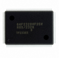
Manufacturer Part Number
DF2328BVF25V
Description
IC H8S MCU FLASH 256K 128QFP
Manufacturer
Renesas Electronics America
Series
H8® H8S/2300r
Datasheets
1.HEWH8E10A.pdf
(19 pages)
2.D12312SVTE25V.pdf
(341 pages)
3.D12322RVF25V.pdf
(1304 pages)
Specifications of DF2328BVF25V
Core Processor
H8S/2000
Core Size
16-Bit
Speed
25MHz
Connectivity
SCI, SmartCard
Peripherals
DMA, POR, PWM, WDT
Number Of I /o
87
Program Memory Size
256KB (256K x 8)
Program Memory Type
FLASH
Ram Size
8K x 8
Voltage - Supply (vcc/vdd)
2.7 V ~ 3.6 V
Data Converters
A/D 8x10b; D/A 2x8b
Oscillator Type
Internal
Operating Temperature
-20°C ~ 75°C
Package / Case
128-QFP
For Use With
EDK2329 - DEV EVALUATION KIT H8S/2329
Lead Free Status / RoHS Status
Lead free / RoHS Compliant
Eeprom Size
-
Other names
HD64F2328BVF25V
Available stocks
Company
Part Number
Manufacturer
Quantity
Price
Company:

Part Number:
DF2328BVF25V
Manufacturer:
Renesas Electronics America
Quantity:
10 000


19.28
All interrupts, including NMI input, are disabled when flash memory is being programmed or
erased (when the P1 or E1 bit is set in FLMCR1, or the P2 or E2 bit is set in FLMCR2), and while
the boot program is executing in boot mode *
There are three reasons for this:
1. Interrupt during programming or erasing might cause a violation of the programming or
2. In the interrupt exception handling sequence during programming or erasing, the vector would
3. If an interrupt occurred during boot program execution, it would not be possible to execute the
For these reasons, in on-board programming mode alone there are conditions for disabling
interrupts, as an exception to the general rule. However, this provision does not guarantee normal
erasing and programming or MCU operation. All requests, including NMI, must therefore be
restricted inside and outside the MCU when programming or erasing flash memory. The NMI
interrupt is also disabled in the error-protection state while the P1 or E1 bit remains set in
FLMCR1, or the P2 or E2 bit remains set in FLMCR2.
Notes: 1. Interrupt requests must be disabled inside and outside the MCU until the programming
erasing algorithm, with the result that normal operation could not be assured.
not be read correctly *
normal boot mode sequence.
2. A RAM area cannot be erased by execution of software in accordance with the erase
3. Block area EB0 includes the vector table. When performing RAM emulation, the
2. The vector may not be read correctly in this case for the following two reasons:
Interrupt Handling when Programming/Erasing Flash Memory
the P2 or E2 bit in FLMCR2 will not cause a transition to program mode or erase
mode. When actually programming a flash memory area, the RAMS bit should be
cleared to 0.
algorithm while flash memory emulation in RAM is being used.
vector table is needed by the overlap RAM.
control program has completed programming.
•
•
If flash memory is read while being programmed or erased (while the P1 or E1 bit
is set in FLMCR1, or the P2 or E2 bit is set in FLMCR2.), correct read data will not
be obtained (undetermined values will be returned).
If the interrupt entry in the vector table has not been programmed yet, interrupt
exception handling will not be executed correctly.
2
, possibly resulting in MCU runaway.
1
, to give priority to the program or erase operation.
Rev.6.00 Sep. 27, 2007 Page 889 of 1268
REJ09B0220-0600
Section 19 ROM
Related parts for DF2328BVF25V
Image
Part Number
Description
Manufacturer
Datasheet
Request
R

Part Number:
Description:
KIT STARTER FOR M16C/29
Manufacturer:
Renesas Electronics America
Datasheet:

Part Number:
Description:
KIT STARTER FOR R8C/2D
Manufacturer:
Renesas Electronics America
Datasheet:

Part Number:
Description:
R0K33062P STARTER KIT
Manufacturer:
Renesas Electronics America
Datasheet:

Part Number:
Description:
KIT STARTER FOR R8C/23 E8A
Manufacturer:
Renesas Electronics America
Datasheet:

Part Number:
Description:
KIT STARTER FOR R8C/25
Manufacturer:
Renesas Electronics America
Datasheet:

Part Number:
Description:
KIT STARTER H8S2456 SHARPE DSPLY
Manufacturer:
Renesas Electronics America
Datasheet:

Part Number:
Description:
KIT STARTER FOR R8C38C
Manufacturer:
Renesas Electronics America
Datasheet:

Part Number:
Description:
KIT STARTER FOR R8C35C
Manufacturer:
Renesas Electronics America
Datasheet:

Part Number:
Description:
KIT STARTER FOR R8CL3AC+LCD APPS
Manufacturer:
Renesas Electronics America
Datasheet:
Part Number:
Description:
KIT STARTER FOR RX610
Manufacturer:
Renesas Electronics America
Datasheet:

Part Number:
Description:
KIT STARTER FOR R32C/118
Manufacturer:
Renesas Electronics America
Datasheet:

Part Number:
Description:
KIT DEV RSK-R8C/26-29
Manufacturer:
Renesas Electronics America
Datasheet:

Part Number:
Description:
KIT STARTER FOR SH7124
Manufacturer:
Renesas Electronics America
Datasheet:

Part Number:
Description:
KIT STARTER FOR H8SX/1622
Manufacturer:
Renesas Electronics America
Datasheet:

Part Number:
Description:
KIT DEV FOR SH7203
Manufacturer:
Renesas Electronics America
Datasheet: