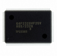
DF2328BVF25V Renesas Electronics America, DF2328BVF25V Datasheet - Page 795

DF2328BVF25V
Manufacturer Part Number
DF2328BVF25V
Description
IC H8S MCU FLASH 256K 128QFP
Manufacturer
Renesas Electronics America
Series
H8® H8S/2300r
Datasheets
1.HEWH8E10A.pdf
(19 pages)
2.D12312SVTE25V.pdf
(341 pages)
3.D12322RVF25V.pdf
(1304 pages)
Specifications of DF2328BVF25V
Core Processor
H8S/2000
Core Size
16-Bit
Speed
25MHz
Connectivity
SCI, SmartCard
Peripherals
DMA, POR, PWM, WDT
Number Of I /o
87
Program Memory Size
256KB (256K x 8)
Program Memory Type
FLASH
Ram Size
8K x 8
Voltage - Supply (vcc/vdd)
2.7 V ~ 3.6 V
Data Converters
A/D 8x10b; D/A 2x8b
Oscillator Type
Internal
Operating Temperature
-20°C ~ 75°C
Package / Case
128-QFP
For Use With
EDK2329 - DEV EVALUATION KIT H8S/2329
Lead Free Status / RoHS Status
Lead free / RoHS Compliant
Eeprom Size
-
Other names
HD64F2328BVF25V
Available stocks
Company
Part Number
Manufacturer
Quantity
Price
Company:
Part Number:
DF2328BVF25V
Manufacturer:
Renesas Electronics America
Quantity:
10 000
- Current page: 795 of 1304
- Download datasheet (8Mb)
• The contents of the CPU’s internal general registers are undefined at this time, so these
• Initial settings must also be made for the other on-chip registers.
• Boot mode can be entered by making the pin settings shown in table 19.9 and executing a
• Boot mode can be cleared by driving the reset pin low, waiting at least 20 states, then setting
• Do not change the mode pin input levels in boot mode.
• If the mode pin input levels are changed (for example, from low to high) during a reset, the
Notes: 1. Mode pins input must satisfy the mode programming setup time (t
19.6.2
When set to user program mode, the chip can program and erase its flash memory by executing a
user program/erase control program. Therefore, on-board reprogramming of the on-chip flash
memory can be carried out by providing on-board means supply of programming data, and storing
a program/erase control program in part of the program area if necessary.
To select user program mode, select a mode that enables the on-chip flash memory (mode 6 or 7).
In this mode, on-chip supporting modules other than flash memory operate as they normally
would in modes 6 and 7.
The flash memory itself cannot be read while the SWE bit is set to 1 to perform programming or
erasing, so the control program that performs programming and erasing should be run in on-chip
RAM or external memory. When the program is located in external memory, an instruction for
programming the flash memory and the following instruction should be located in on-chip RAM.
registers must be initialized immediately after branching to the programming control program.
In particular, since the stack pointer (SP) is used implicitly in subroutine calls, etc., a stack area
must be specified for use by the programming control program.
reset-start.
the mode pins, and executing reset release *
overflow reset.
state of ports with multiplexed address functions and bus control output pins (AS, RD, HWR)
will change according to the change in the microcomputer’s operating mode *
Therefore, care must be taken to make pin settings to prevent these pins from becoming output
signal pins during a reset, or to prevent collision with signals outside the microcomputer.
2. See section 9, I/O Ports.
User Program Mode
respect to the reset release timing.
1
. Boot mode can also be cleared by a WDT
Rev.6.00 Sep. 27, 2007 Page 763 of 1268
MDS
REJ09B0220-0600
2
Section 19 ROM
= 200 ns) with
.
Related parts for DF2328BVF25V
Image
Part Number
Description
Manufacturer
Datasheet
Request
R

Part Number:
Description:
KIT STARTER FOR M16C/29
Manufacturer:
Renesas Electronics America
Datasheet:

Part Number:
Description:
KIT STARTER FOR R8C/2D
Manufacturer:
Renesas Electronics America
Datasheet:

Part Number:
Description:
R0K33062P STARTER KIT
Manufacturer:
Renesas Electronics America
Datasheet:

Part Number:
Description:
KIT STARTER FOR R8C/23 E8A
Manufacturer:
Renesas Electronics America
Datasheet:

Part Number:
Description:
KIT STARTER FOR R8C/25
Manufacturer:
Renesas Electronics America
Datasheet:

Part Number:
Description:
KIT STARTER H8S2456 SHARPE DSPLY
Manufacturer:
Renesas Electronics America
Datasheet:

Part Number:
Description:
KIT STARTER FOR R8C38C
Manufacturer:
Renesas Electronics America
Datasheet:

Part Number:
Description:
KIT STARTER FOR R8C35C
Manufacturer:
Renesas Electronics America
Datasheet:

Part Number:
Description:
KIT STARTER FOR R8CL3AC+LCD APPS
Manufacturer:
Renesas Electronics America
Datasheet:

Part Number:
Description:
KIT STARTER FOR RX610
Manufacturer:
Renesas Electronics America
Datasheet:

Part Number:
Description:
KIT STARTER FOR R32C/118
Manufacturer:
Renesas Electronics America
Datasheet:

Part Number:
Description:
KIT DEV RSK-R8C/26-29
Manufacturer:
Renesas Electronics America
Datasheet:

Part Number:
Description:
KIT STARTER FOR SH7124
Manufacturer:
Renesas Electronics America
Datasheet:

Part Number:
Description:
KIT STARTER FOR H8SX/1622
Manufacturer:
Renesas Electronics America
Datasheet:

Part Number:
Description:
KIT DEV FOR SH7203
Manufacturer:
Renesas Electronics America
Datasheet:


