DF2328BVF25V Renesas Electronics America, DF2328BVF25V Datasheet - Page 188
DF2328BVF25V
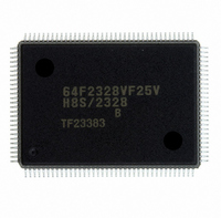
Manufacturer Part Number
DF2328BVF25V
Description
IC H8S MCU FLASH 256K 128QFP
Manufacturer
Renesas Electronics America
Series
H8® H8S/2300r
Datasheets
1.HEWH8E10A.pdf
(19 pages)
2.D12312SVTE25V.pdf
(341 pages)
3.D12322RVF25V.pdf
(1304 pages)
Specifications of DF2328BVF25V
Core Processor
H8S/2000
Core Size
16-Bit
Speed
25MHz
Connectivity
SCI, SmartCard
Peripherals
DMA, POR, PWM, WDT
Number Of I /o
87
Program Memory Size
256KB (256K x 8)
Program Memory Type
FLASH
Ram Size
8K x 8
Voltage - Supply (vcc/vdd)
2.7 V ~ 3.6 V
Data Converters
A/D 8x10b; D/A 2x8b
Oscillator Type
Internal
Operating Temperature
-20°C ~ 75°C
Package / Case
128-QFP
For Use With
EDK2329 - DEV EVALUATION KIT H8S/2329
Lead Free Status / RoHS Status
Lead free / RoHS Compliant
Eeprom Size
-
Other names
HD64F2328BVF25V
Available stocks
Company
Part Number
Manufacturer
Quantity
Price
Company:

Part Number:
DF2328BVF25V
Manufacturer:
Renesas Electronics America
Quantity:
10 000


Section 6 Bus Controller
Bit 3
BRSTS0
0
1
Bits 2 to 0—RAM Type Select (RMTS2 to RMTS0): These bits select the memory interface for
areas 2 to 5 in advanced mode.
When DRAM space is selected, the relevant area is designated as a DRAM interface area. In the
H8S/2321 these bits are reserved and should only be written with 0.
Bit 2
RMTS2
0
1
The LCAS pin is used for the LCAS signal on the 2-CAS DRAM interface. If it is wished to use
BREQO output and WAIT input when using the LCAS signal, it is possible to switch to the P5
pin by means of the BREQOPS bit in PFCR2. For details, see section 9.6, Port 5 and section 9.13,
Port F.
Note: This note applies to the H8S/2323 only. If all areas selected as DRAM space are 8-bit
RMTS2
0
Rev.6.00 Sep. 27, 2007 Page 156 of 1268
REJ09B0220-0600
space, the PF
PF
should be designated as 16-bit bus space. The RAS down mode cannot be used in this
case. Sample settings are shown below.
2
RMTS1
0
1
Bit 1
RMTS1
0
1
—
is used as the WAIT pin on the H8S/2323 only, normal space other than DRAM space
Description
Max. 4 words in burst access
Max. 8 words in burst access
2
RMTS0
0
1
0
1
pin can be used as an I/O port, or as the BREQ0 or WAIT pin. However, if
Bit 0
RMTS0
0
1
0
1
—
Area 5
Normal space
Normal space
(16-bit bus)
Normal space
(16-bit bus)
DRAM space
(8-bit bus)
Description
Area 5
Normal space
Normal space
Normal space
DRAM space
—
Area 4
Area 4
Area 3
DRAM space
(8-bit bus)
DRAM space
Area 3
Area 2
DRAM space
(8-bit bus)
Area 2
DRAM space
(Initial value)
3
Related parts for DF2328BVF25V
Image
Part Number
Description
Manufacturer
Datasheet
Request
R

Part Number:
Description:
KIT STARTER FOR M16C/29
Manufacturer:
Renesas Electronics America
Datasheet:

Part Number:
Description:
KIT STARTER FOR R8C/2D
Manufacturer:
Renesas Electronics America
Datasheet:

Part Number:
Description:
R0K33062P STARTER KIT
Manufacturer:
Renesas Electronics America
Datasheet:

Part Number:
Description:
KIT STARTER FOR R8C/23 E8A
Manufacturer:
Renesas Electronics America
Datasheet:

Part Number:
Description:
KIT STARTER FOR R8C/25
Manufacturer:
Renesas Electronics America
Datasheet:

Part Number:
Description:
KIT STARTER H8S2456 SHARPE DSPLY
Manufacturer:
Renesas Electronics America
Datasheet:

Part Number:
Description:
KIT STARTER FOR R8C38C
Manufacturer:
Renesas Electronics America
Datasheet:

Part Number:
Description:
KIT STARTER FOR R8C35C
Manufacturer:
Renesas Electronics America
Datasheet:

Part Number:
Description:
KIT STARTER FOR R8CL3AC+LCD APPS
Manufacturer:
Renesas Electronics America
Datasheet:
Part Number:
Description:
KIT STARTER FOR RX610
Manufacturer:
Renesas Electronics America
Datasheet:

Part Number:
Description:
KIT STARTER FOR R32C/118
Manufacturer:
Renesas Electronics America
Datasheet:

Part Number:
Description:
KIT DEV RSK-R8C/26-29
Manufacturer:
Renesas Electronics America
Datasheet:

Part Number:
Description:
KIT STARTER FOR SH7124
Manufacturer:
Renesas Electronics America
Datasheet:

Part Number:
Description:
KIT STARTER FOR H8SX/1622
Manufacturer:
Renesas Electronics America
Datasheet:

Part Number:
Description:
KIT DEV FOR SH7203
Manufacturer:
Renesas Electronics America
Datasheet: