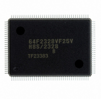
DF2328BVF25V Renesas Electronics America, DF2328BVF25V Datasheet - Page 1009

DF2328BVF25V
Manufacturer Part Number
DF2328BVF25V
Description
IC H8S MCU FLASH 256K 128QFP
Manufacturer
Renesas Electronics America
Series
H8® H8S/2300r
Datasheets
1.HEWH8E10A.pdf
(19 pages)
2.D12312SVTE25V.pdf
(341 pages)
3.D12322RVF25V.pdf
(1304 pages)
Specifications of DF2328BVF25V
Core Processor
H8S/2000
Core Size
16-Bit
Speed
25MHz
Connectivity
SCI, SmartCard
Peripherals
DMA, POR, PWM, WDT
Number Of I /o
87
Program Memory Size
256KB (256K x 8)
Program Memory Type
FLASH
Ram Size
8K x 8
Voltage - Supply (vcc/vdd)
2.7 V ~ 3.6 V
Data Converters
A/D 8x10b; D/A 2x8b
Oscillator Type
Internal
Operating Temperature
-20°C ~ 75°C
Package / Case
128-QFP
For Use With
EDK2329 - DEV EVALUATION KIT H8S/2329
Lead Free Status / RoHS Status
Lead free / RoHS Compliant
Eeprom Size
-
Other names
HD64F2328BVF25V
Available stocks
Company
Part Number
Manufacturer
Quantity
Price
Company:
Part Number:
DF2328BVF25V
Manufacturer:
Renesas Electronics America
Quantity:
10 000
- Current page: 1009 of 1304
- Download datasheet (8Mb)
22.2.6
Table 22.22 Flash Memory Characteristics
Conditions: V
Item
Programming time
Erase time
Rewrite times
Data hold time
Programming Wait time after SWE bit setting
Erasing
*
Flash Memory Characteristics
1
*
3
0 V, T
specifications), T
wide-range specifications)
Wait time after PSU bit setting
Wait time after P bit setting
Wait time after P bit clearing
Wait time after PSU bit clearing
Wait time after PV bit setting
Wait time after H'FF dummy write
Wait time after PV bit clearing
Wait time after SWE bit clearing
Maximum number of writes
Wait time after SWE bit setting
Wait time after ESU bit setting
Wait time after E bit setting
Wait time after E bit clearing
Wait time after ESU bit clearing
Wait time after EV bit setting
Wait time after H'FF dummy write
Wait time after EV bit clearing
Wait time after SWE bit clearing
Maximum number of erases
*
CC
6
*
1
= 3.0 V to 3.6 V, AV
*
2
a
*
= 0°C to +75°C (program/erase operating temperature range: regular
4
a
= 0°C to +85°C (program/erase operating temperature range:
*
*
*
*
1
1
*
*
1
*
*
CC
1
1
1
*
1
*
1
*
*
*
*
*
*
*
*
4
6
1
4
1
1
1
*
*
1
1
6
= 3.0 V to 3.6 V, V
*
*
1
1
1
1
*
*
1
1
Symbol
t
t
N
t
x
y
z
α
β
γ
ε
η
θ
N
x
y
z
α
β
γ
ε
η
θ
N
P
E
DRP
WEC
*
9
(z1) —
(z2) —
(z3) —
Rev.6.00 Sep. 27, 2007 Page 977 of 1268
Min
—
—
100 *
10
1
50
5
5
4
2
2
100
—
1
100
—
10
10
20
2
4
100
—
7
ref
Section 22 Electrical Characteristics
Typ
10
50
10000 *
—
—
—
—
—
—
—
—
—
—
—
—
—
—
—
—
—
—
—
—
—
—
—
= 3.0 V to AV
8
Max
200
1000
—
—
—
—
30
200
10
—
—
—
—
—
—
1000 *
—
—
10
—
—
—
—
—
—
100
5
Unit
ms/
128 bytes
ms/block
Times
year
μs
μs
μs
μs
μs
μs
μs
μs
μs
μs
μs
Times
μs
μs
ms
μs
μs
μs
μs
μs
μs
Times
CC
REJ09B0220-0600
, V
SS
= AV
Test
Conditions
1 ≤ n ≤ 6
7 ≤ n ≤ 1000
Wait time for
additional
writing
Wait time for
erase time
SS
=
Related parts for DF2328BVF25V
Image
Part Number
Description
Manufacturer
Datasheet
Request
R

Part Number:
Description:
KIT STARTER FOR M16C/29
Manufacturer:
Renesas Electronics America
Datasheet:

Part Number:
Description:
KIT STARTER FOR R8C/2D
Manufacturer:
Renesas Electronics America
Datasheet:

Part Number:
Description:
R0K33062P STARTER KIT
Manufacturer:
Renesas Electronics America
Datasheet:

Part Number:
Description:
KIT STARTER FOR R8C/23 E8A
Manufacturer:
Renesas Electronics America
Datasheet:

Part Number:
Description:
KIT STARTER FOR R8C/25
Manufacturer:
Renesas Electronics America
Datasheet:

Part Number:
Description:
KIT STARTER H8S2456 SHARPE DSPLY
Manufacturer:
Renesas Electronics America
Datasheet:

Part Number:
Description:
KIT STARTER FOR R8C38C
Manufacturer:
Renesas Electronics America
Datasheet:

Part Number:
Description:
KIT STARTER FOR R8C35C
Manufacturer:
Renesas Electronics America
Datasheet:

Part Number:
Description:
KIT STARTER FOR R8CL3AC+LCD APPS
Manufacturer:
Renesas Electronics America
Datasheet:

Part Number:
Description:
KIT STARTER FOR RX610
Manufacturer:
Renesas Electronics America
Datasheet:

Part Number:
Description:
KIT STARTER FOR R32C/118
Manufacturer:
Renesas Electronics America
Datasheet:

Part Number:
Description:
KIT DEV RSK-R8C/26-29
Manufacturer:
Renesas Electronics America
Datasheet:

Part Number:
Description:
KIT STARTER FOR SH7124
Manufacturer:
Renesas Electronics America
Datasheet:

Part Number:
Description:
KIT STARTER FOR H8SX/1622
Manufacturer:
Renesas Electronics America
Datasheet:

Part Number:
Description:
KIT DEV FOR SH7203
Manufacturer:
Renesas Electronics America
Datasheet:


