DF2328BVF25V Renesas Electronics America, DF2328BVF25V Datasheet - Page 885
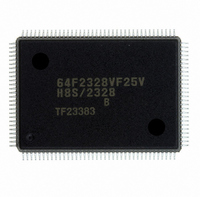
DF2328BVF25V
Manufacturer Part Number
DF2328BVF25V
Description
IC H8S MCU FLASH 256K 128QFP
Manufacturer
Renesas Electronics America
Series
H8® H8S/2300r
Datasheets
1.HEWH8E10A.pdf
(19 pages)
2.D12312SVTE25V.pdf
(341 pages)
3.D12322RVF25V.pdf
(1304 pages)
Specifications of DF2328BVF25V
Core Processor
H8S/2000
Core Size
16-Bit
Speed
25MHz
Connectivity
SCI, SmartCard
Peripherals
DMA, POR, PWM, WDT
Number Of I /o
87
Program Memory Size
256KB (256K x 8)
Program Memory Type
FLASH
Ram Size
8K x 8
Voltage - Supply (vcc/vdd)
2.7 V ~ 3.6 V
Data Converters
A/D 8x10b; D/A 2x8b
Oscillator Type
Internal
Operating Temperature
-20°C ~ 75°C
Package / Case
128-QFP
For Use With
EDK2329 - DEV EVALUATION KIT H8S/2329
Lead Free Status / RoHS Status
Lead free / RoHS Compliant
Eeprom Size
-
Other names
HD64F2328BVF25V
Available stocks
Company
Part Number
Manufacturer
Quantity
Price
Company:

Part Number:
DF2328BVF25V
Manufacturer:
Renesas Electronics America
Quantity:
10 000


• User program mode
1. Initial state
3. Flash memory initialization
(1) The FWE assessment program that confirms
that the FWE pin has been driven high, and (2)
the program that will transfer the programming/
erase control program to on-chip RAM should be
written into the flash memory by the user
beforehand. (3) The programming/erase control
program should be prepared in the host or in the
flash memory.
The programming/erase program in RAM is
executed, and the flash memory is initialized (to
H'FF). Erasing can be performed in block units,
but not in byte units.
Chip
Chip
Application program
Transfer program
Transfer program
FWE assessment
FWE assessment
Flash memory
Flash memory
Flash memory
Boot program
Boot program
(old version)
program
program
erase
erase control program
New application
New application
Programming/
program
program
Host
Host
Figure 19.62 User Program Mode (Example)
erase control program
Programming/
RAM
RAM
SCI
SCI
2. Programming/erase control program transfer
4. Writing new application program
Chip
Chip
When the FWE pin is driven high, user software
confirms this fact, executes the transfer program
in the flash memory, and transfers the
programming/erase control program to RAM.
Next, the new application program in the host is
written into the erased flash memory blocks. Do
not write to unerased blocks.
Application program
Rev.6.00 Sep. 27, 2007 Page 853 of 1268
Transfer program
New application
FWE assessment
FWE assessment
Transfer program
Flash memory
Flash memory
Boot program
Boot program
(old version)
program
program
program
New application
program
Host
Host
erase control program
erase control program
Programming/
Programming/
Program execution state
RAM
RAM
REJ09B0220-0600
SCI
SCI
Section 19 ROM
Related parts for DF2328BVF25V
Image
Part Number
Description
Manufacturer
Datasheet
Request
R

Part Number:
Description:
KIT STARTER FOR M16C/29
Manufacturer:
Renesas Electronics America
Datasheet:

Part Number:
Description:
KIT STARTER FOR R8C/2D
Manufacturer:
Renesas Electronics America
Datasheet:

Part Number:
Description:
R0K33062P STARTER KIT
Manufacturer:
Renesas Electronics America
Datasheet:

Part Number:
Description:
KIT STARTER FOR R8C/23 E8A
Manufacturer:
Renesas Electronics America
Datasheet:

Part Number:
Description:
KIT STARTER FOR R8C/25
Manufacturer:
Renesas Electronics America
Datasheet:

Part Number:
Description:
KIT STARTER H8S2456 SHARPE DSPLY
Manufacturer:
Renesas Electronics America
Datasheet:

Part Number:
Description:
KIT STARTER FOR R8C38C
Manufacturer:
Renesas Electronics America
Datasheet:

Part Number:
Description:
KIT STARTER FOR R8C35C
Manufacturer:
Renesas Electronics America
Datasheet:

Part Number:
Description:
KIT STARTER FOR R8CL3AC+LCD APPS
Manufacturer:
Renesas Electronics America
Datasheet:
Part Number:
Description:
KIT STARTER FOR RX610
Manufacturer:
Renesas Electronics America
Datasheet:

Part Number:
Description:
KIT STARTER FOR R32C/118
Manufacturer:
Renesas Electronics America
Datasheet:

Part Number:
Description:
KIT DEV RSK-R8C/26-29
Manufacturer:
Renesas Electronics America
Datasheet:

Part Number:
Description:
KIT STARTER FOR SH7124
Manufacturer:
Renesas Electronics America
Datasheet:

Part Number:
Description:
KIT STARTER FOR H8SX/1622
Manufacturer:
Renesas Electronics America
Datasheet:

Part Number:
Description:
KIT DEV FOR SH7203
Manufacturer:
Renesas Electronics America
Datasheet: