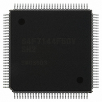
HD64F7144F50V Renesas Electronics America, HD64F7144F50V Datasheet - Page 565

HD64F7144F50V
Manufacturer Part Number
HD64F7144F50V
Description
IC SUPERH MCU FLASH 256K 112QFP
Manufacturer
Renesas Electronics America
Series
SuperH® SH7144r
Specifications of HD64F7144F50V
Core Processor
SH-2
Core Size
32-Bit
Speed
50MHz
Connectivity
EBI/EMI, I²C, SCI
Peripherals
DMA, POR, PWM, WDT
Number Of I /o
74
Program Memory Size
256KB (256K x 8)
Program Memory Type
FLASH
Ram Size
8K x 8
Voltage - Supply (vcc/vdd)
3 V ~ 3.6 V
Data Converters
A/D 8x10b
Oscillator Type
Internal
Operating Temperature
-20°C ~ 75°C
Package / Case
112-QFP
For Use With
HS0005KCU11H - EMULATOR E10A-USB H8S(X),SH2(A)EDK7145 - DEV EVALUATION KIT SH7145
Lead Free Status / RoHS Status
Lead free / RoHS Compliant
Eeprom Size
-
Available stocks
Company
Part Number
Manufacturer
Quantity
Price
Company:
Part Number:
HD64F7144F50V
Manufacturer:
RENESAS
Quantity:
450
Company:
Part Number:
HD64F7144F50V
Manufacturer:
Renesas Electronics America
Quantity:
10 000
Part Number:
HD64F7144F50V
Manufacturer:
RENESAS/瑞萨
Quantity:
20 000
- Current page: 565 of 932
- Download datasheet (6Mb)
In the slave transmit mode, the slave device transmits data while the master device outputs the
receive clock and returns acknowledgements of reception. The following description gives the
procedures for and operations of transmitting in slave transmit mode.
1. Perform initialization of slave receive mode and wait for slave address reception.
2. When the slave address matches the address in the first frame following the start condition
3. After the IRIC flag is cleared to 0, the transmit data is written to ICDR. In this case, the
4. The master device drives SDA to low at the 9th cycle of the transfer frame and returns the
5. To continue with the transmission, write the next data for transmission to ICDR. In this case,
6. Clear the IRIC flag to 0.
7. To end the transmission, clear the ACKE bit in ICCR and the acknowledge bit stored in the
8. For the next address reception, clear the TRS bit to 0 and enter slave receive mode.
9. To release SDA on the slave side, dummy read ICDR.
detection, the slave device drives SDA to low at the 9th cycle of the clock and returns
acknowledgement. When the 8th bit of data (R/W) is 1, the TRS bit is set to 1 and slave
transmit mode is automatically entered. The IRIC flag is set to 1 at the rising edge of the 9th
cycle of the clock. At this time, if the IEIC bit is set to 1, an interrupt request is generated for
the CPU. The ICDRE flag is set to 1. The slave device keeps SCL low to prevent the master
device from outputting the next transmit clock from the falling edge of the 9th cycle of the
transmit clock until data is written to ICDR.
ICDRE flag is cleared to 0. The written data is transferred to ICDRS, and the ICDRE and IRIC
flags are again set to 1. The slave device sequentially transmits the data transferred to ICDRS,
on the basis of the clock from the master device.
To detect the completion of transmission, clear the IRIC flag to 0. After writing the ICDR
register, sequentially clear the IRIC flag so that no other process is inserted.
acknowledgement. Since the acknowledgement is stored in the ACKB bit in ICSR, it can be
checked whether transfer operation is performed normally. One frame of data transmission is
completed and the IRIC flag is set to 1 at the rising edge of the 9th cycle of the transmit clock.
When the ICDRE flag is 0, data written to the ICDR is transferred to ICDRS and one frame of
data transmission is started, and then the ICDRE and IRIC flags are again set to 1. If the
ICDRE flag is set to 1, SCL is kept low from the falling edge of the 9th cycle of the transmit
clock until the data is written to the ICDR.
the ICDRE flag is cleared to 0. To detect the completion of transmission, clear the IRIC flag to
0. Perform the ICDR register writing and the IRIC flag clearing sequentially so that no other
process is inserted.
Transmission can be continued by repeating steps 4 and 5.
ACKB bit to 0.
Rev.4.00 Mar. 27, 2008 Page 519 of 882
14. I
2
C Bus Interface (IIC) Option
REJ09B0108-0400
Related parts for HD64F7144F50V
Image
Part Number
Description
Manufacturer
Datasheet
Request
R

Part Number:
Description:
KIT STARTER FOR M16C/29
Manufacturer:
Renesas Electronics America
Datasheet:

Part Number:
Description:
KIT STARTER FOR R8C/2D
Manufacturer:
Renesas Electronics America
Datasheet:

Part Number:
Description:
R0K33062P STARTER KIT
Manufacturer:
Renesas Electronics America
Datasheet:

Part Number:
Description:
KIT STARTER FOR R8C/23 E8A
Manufacturer:
Renesas Electronics America
Datasheet:

Part Number:
Description:
KIT STARTER FOR R8C/25
Manufacturer:
Renesas Electronics America
Datasheet:

Part Number:
Description:
KIT STARTER H8S2456 SHARPE DSPLY
Manufacturer:
Renesas Electronics America
Datasheet:

Part Number:
Description:
KIT STARTER FOR R8C38C
Manufacturer:
Renesas Electronics America
Datasheet:

Part Number:
Description:
KIT STARTER FOR R8C35C
Manufacturer:
Renesas Electronics America
Datasheet:

Part Number:
Description:
KIT STARTER FOR R8CL3AC+LCD APPS
Manufacturer:
Renesas Electronics America
Datasheet:

Part Number:
Description:
KIT STARTER FOR RX610
Manufacturer:
Renesas Electronics America
Datasheet:

Part Number:
Description:
KIT STARTER FOR R32C/118
Manufacturer:
Renesas Electronics America
Datasheet:

Part Number:
Description:
KIT DEV RSK-R8C/26-29
Manufacturer:
Renesas Electronics America
Datasheet:

Part Number:
Description:
KIT STARTER FOR SH7124
Manufacturer:
Renesas Electronics America
Datasheet:

Part Number:
Description:
KIT STARTER FOR H8SX/1622
Manufacturer:
Renesas Electronics America
Datasheet:


