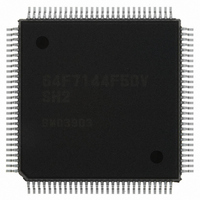
HD64F7144F50V Renesas Electronics America, HD64F7144F50V Datasheet - Page 17

HD64F7144F50V
Manufacturer Part Number
HD64F7144F50V
Description
IC SUPERH MCU FLASH 256K 112QFP
Manufacturer
Renesas Electronics America
Series
SuperH® SH7144r
Specifications of HD64F7144F50V
Core Processor
SH-2
Core Size
32-Bit
Speed
50MHz
Connectivity
EBI/EMI, I²C, SCI
Peripherals
DMA, POR, PWM, WDT
Number Of I /o
74
Program Memory Size
256KB (256K x 8)
Program Memory Type
FLASH
Ram Size
8K x 8
Voltage - Supply (vcc/vdd)
3 V ~ 3.6 V
Data Converters
A/D 8x10b
Oscillator Type
Internal
Operating Temperature
-20°C ~ 75°C
Package / Case
112-QFP
For Use With
HS0005KCU11H - EMULATOR E10A-USB H8S(X),SH2(A)EDK7145 - DEV EVALUATION KIT SH7145
Lead Free Status / RoHS Status
Lead free / RoHS Compliant
Eeprom Size
-
Available stocks
Company
Part Number
Manufacturer
Quantity
Price
Company:
Part Number:
HD64F7144F50V
Manufacturer:
RENESAS
Quantity:
450
Company:
Part Number:
HD64F7144F50V
Manufacturer:
Renesas Electronics America
Quantity:
10 000
Part Number:
HD64F7144F50V
Manufacturer:
RENESAS/瑞萨
Quantity:
20 000
- Current page: 17 of 932
- Download datasheet (6Mb)
11.6 Operation Timing..............................................................................................................313
11.7 Usage Notes ......................................................................................................................321
11.8 MTU Output Pin Initialization ..........................................................................................336
11.9 Port Output Enable (POE).................................................................................................368
11.5.2 DTC/DMAC Activation.......................................................................................312
11.5.3 A/D Converter Activation....................................................................................312
11.6.1 Input/Output Timing ............................................................................................313
11.6.2 Interrupt Signal Timing........................................................................................318
11.7.1 Module Standby Mode Setting.............................................................................321
11.7.2 Input Clock Restrictions.......................................................................................321
11.7.3 Caution on Period Setting ....................................................................................322
11.7.4 Contention between TCNT Write and Clear Operations .....................................322
11.7.5 Contention between TCNT Write and Increment Operations..............................323
11.7.6 Contention between TGR Write and Compare Match .........................................324
11.7.7 Contention between Buffer Register Write and Compare Match ........................325
11.7.8 Contention between TGR Read and Input Capture..............................................326
11.7.9 Contention between TGR Write and Input Capture.............................................327
11.7.10 Contention between Buffer Register Write and Input Capture ............................328
11.7.11 TCNT2 Write and Overflow/Underflow Contention in Cascade Connection......328
11.7.12 Counter Value during Complementary PWM Mode Stop ...................................330
11.7.13 Buffer Operation Setting in Complementary PWM Mode...................................330
11.7.14 Reset Sync PWM Mode Buffer Operation and Compare Match Flag .................331
11.7.15 Overflow Flags in Reset Synchronous PWM Mode ............................................332
11.7.16 Contention between Overflow/Underflow and Counter Clearing........................333
11.7.17 Contention between TCNT Write and Overflow/Underflow...............................334
11.7.18 Cautions on Transition from Normal Operation or PWM Mode 1 to
11.7.19 Output Level in Complementary PWM Mode and Reset-Synchronous
11.7.20 Interrupts in Module Standby Mode ....................................................................335
11.7.21 Simultaneous Capture of TCNT_1 and TCNT_2 in Cascade Connection...........335
11.7.22 Note on Buffer Operation Setting ........................................................................335
11.8.1 Operating Modes..................................................................................................336
11.8.2 Reset Start Operation ...........................................................................................336
11.8.3 Operation in Case of Re-Setting Due to Error During Operation, Etc. ................337
11.8.4 Overview of Initialization Procedures and Mode Transitions in Case of
11.9.1 Features................................................................................................................368
11.9.2 Pin Configuration.................................................................................................370
11.9.3 Register Descriptions ...........................................................................................370
Reset-Synchronous PWM Mode..........................................................................334
PWM Mode..........................................................................................................335
Error during Operation, etc. .................................................................................338
Rev.4.00 Mar. 27, 2008, Page xv of xliv
REJ09B0108-0400
Related parts for HD64F7144F50V
Image
Part Number
Description
Manufacturer
Datasheet
Request
R

Part Number:
Description:
KIT STARTER FOR M16C/29
Manufacturer:
Renesas Electronics America
Datasheet:

Part Number:
Description:
KIT STARTER FOR R8C/2D
Manufacturer:
Renesas Electronics America
Datasheet:

Part Number:
Description:
R0K33062P STARTER KIT
Manufacturer:
Renesas Electronics America
Datasheet:

Part Number:
Description:
KIT STARTER FOR R8C/23 E8A
Manufacturer:
Renesas Electronics America
Datasheet:

Part Number:
Description:
KIT STARTER FOR R8C/25
Manufacturer:
Renesas Electronics America
Datasheet:

Part Number:
Description:
KIT STARTER H8S2456 SHARPE DSPLY
Manufacturer:
Renesas Electronics America
Datasheet:

Part Number:
Description:
KIT STARTER FOR R8C38C
Manufacturer:
Renesas Electronics America
Datasheet:

Part Number:
Description:
KIT STARTER FOR R8C35C
Manufacturer:
Renesas Electronics America
Datasheet:

Part Number:
Description:
KIT STARTER FOR R8CL3AC+LCD APPS
Manufacturer:
Renesas Electronics America
Datasheet:

Part Number:
Description:
KIT STARTER FOR RX610
Manufacturer:
Renesas Electronics America
Datasheet:

Part Number:
Description:
KIT STARTER FOR R32C/118
Manufacturer:
Renesas Electronics America
Datasheet:

Part Number:
Description:
KIT DEV RSK-R8C/26-29
Manufacturer:
Renesas Electronics America
Datasheet:

Part Number:
Description:
KIT STARTER FOR SH7124
Manufacturer:
Renesas Electronics America
Datasheet:

Part Number:
Description:
KIT STARTER FOR H8SX/1622
Manufacturer:
Renesas Electronics America
Datasheet:


