HD64F7144F50V Renesas Electronics America, HD64F7144F50V Datasheet - Page 216
HD64F7144F50V
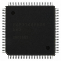
Manufacturer Part Number
HD64F7144F50V
Description
IC SUPERH MCU FLASH 256K 112QFP
Manufacturer
Renesas Electronics America
Series
SuperH® SH7144r
Specifications of HD64F7144F50V
Core Processor
SH-2
Core Size
32-Bit
Speed
50MHz
Connectivity
EBI/EMI, I²C, SCI
Peripherals
DMA, POR, PWM, WDT
Number Of I /o
74
Program Memory Size
256KB (256K x 8)
Program Memory Type
FLASH
Ram Size
8K x 8
Voltage - Supply (vcc/vdd)
3 V ~ 3.6 V
Data Converters
A/D 8x10b
Oscillator Type
Internal
Operating Temperature
-20°C ~ 75°C
Package / Case
112-QFP
For Use With
HS0005KCU11H - EMULATOR E10A-USB H8S(X),SH2(A)EDK7145 - DEV EVALUATION KIT SH7145
Lead Free Status / RoHS Status
Lead free / RoHS Compliant
Eeprom Size
-
Available stocks
Company
Part Number
Manufacturer
Quantity
Price
Company:

Part Number:
HD64F7144F50V
Manufacturer:
RENESAS
Quantity:
450
Company:
Part Number:
HD64F7144F50V
Manufacturer:
Renesas Electronics America
Quantity:
10 000
Part Number:
HD64F7144F50V
Manufacturer:
RENESAS/瑞萨
Quantity:
20 000


10. Direct Memory Access Controller (DMAC)
10.3
The DMAC has the following registers. The DMAC has a total of 17 registers. Each channel has
four control registers. One other control register is shared by all channels. For register address and
their states in each operating mode, refer to section 25, List of Registers.
• DMA source address register_0 (SAR_0)
• DMA destination address register_0 (DAR_0)
• DMA transfer count register_0 (DMATCR_0)
• DMA channel control register_0 (CHCR_0)
• DMA source address register_1 (SAR_1)
• DMA destination address register_1 (DAR_1)
• DMA transfer count register_1 (DMATCR_1)
• DMA channel control register_1 (CHCR_1)
• DMA source address register_2 (SAR_2)
• DMA destination address register_2 (DAR_2)
• DMA transfer count register_2 (DMATCR_2)
• DMA channel control register_2 (CHCR_2)
• DMA source address register_3 (SAR_3)
• DMA destination address register_3 (DAR_3)
• DMA transfer count register_3 (DMATCR_3)
• DMA channel control register_3 (CHCR_3)
• DMA operation register (DMAOR)
10.3.1
DMA source address registers_0 to 3 (SAR_0 to SAR_3) are 32-bit readable/writable registers
that specify the source address of a DMA transfer. These registers have a count function, and
during a DMA transfer, they indicate the next source address. In single-address mode, SAR values
are ignored when a device with DACK has been specified as the transfer source.
Specify a 16-bit or 32-bit boundary address when doing 16-bit or 32-bit data transfers. Operation
cannot be guaranteed on any other addresses.
When this register is accessed in 16 bits, the value of another 16 bits that are not accessed is
retained.
The initial value of SAR is undefined.
Rev.4.00 Mar. 27, 2008 Page 170 of 882
REJ09B0108-0400
Register Descriptions
DMA Source Address Registers_0 to 3 (SAR_0 to SAR_3)
Related parts for HD64F7144F50V
Image
Part Number
Description
Manufacturer
Datasheet
Request
R


Part Number:
Description:
KIT STARTER FOR M16C/29
Manufacturer:
Renesas Electronics America
Datasheet:

Part Number:
Description:
KIT STARTER FOR R8C/2D
Manufacturer:
Renesas Electronics America
Datasheet:

Part Number:
Description:
R0K33062P STARTER KIT
Manufacturer:
Renesas Electronics America
Datasheet:

Part Number:
Description:
KIT STARTER FOR R8C/23 E8A
Manufacturer:
Renesas Electronics America
Datasheet:

Part Number:
Description:
KIT STARTER FOR R8C/25
Manufacturer:
Renesas Electronics America
Datasheet:

Part Number:
Description:
KIT STARTER H8S2456 SHARPE DSPLY
Manufacturer:
Renesas Electronics America
Datasheet:

Part Number:
Description:
KIT STARTER FOR R8C38C
Manufacturer:
Renesas Electronics America
Datasheet:

Part Number:
Description:
KIT STARTER FOR R8C35C
Manufacturer:
Renesas Electronics America
Datasheet:

Part Number:
Description:
KIT STARTER FOR R8CL3AC+LCD APPS
Manufacturer:
Renesas Electronics America
Datasheet:
Part Number:
Description:
KIT STARTER FOR RX610
Manufacturer:
Renesas Electronics America
Datasheet:

Part Number:
Description:
KIT STARTER FOR R32C/118
Manufacturer:
Renesas Electronics America
Datasheet:

Part Number:
Description:
KIT DEV RSK-R8C/26-29
Manufacturer:
Renesas Electronics America
Datasheet:

Part Number:
Description:
KIT STARTER FOR SH7124
Manufacturer:
Renesas Electronics America
Datasheet:

Part Number:
Description:
KIT STARTER FOR H8SX/1622
Manufacturer:
Renesas Electronics America
Datasheet: