HD64F7144F50V Renesas Electronics America, HD64F7144F50V Datasheet - Page 299
HD64F7144F50V
Manufacturer Part Number
HD64F7144F50V
Description
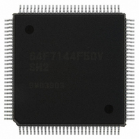
IC SUPERH MCU FLASH 256K 112QFP
Manufacturer
Renesas Electronics America
Series
SuperH® SH7144r
Specifications of HD64F7144F50V
Core Processor
SH-2
Core Size
32-Bit
Speed
50MHz
Connectivity
EBI/EMI, I²C, SCI
Peripherals
DMA, POR, PWM, WDT
Number Of I /o
74
Program Memory Size
256KB (256K x 8)
Program Memory Type
FLASH
Ram Size
8K x 8
Voltage - Supply (vcc/vdd)
3 V ~ 3.6 V
Data Converters
A/D 8x10b
Oscillator Type
Internal
Operating Temperature
-20°C ~ 75°C
Package / Case
112-QFP
For Use With
HS0005KCU11H - EMULATOR E10A-USB H8S(X),SH2(A)EDK7145 - DEV EVALUATION KIT SH7145
Lead Free Status / RoHS Status
Lead free / RoHS Compliant
Eeprom Size
-
Available stocks
Company
Part Number
Manufacturer
Quantity
Price
Company:

Part Number:
HD64F7144F50V
Manufacturer:
RENESAS
Quantity:
450
Company:
Part Number:
HD64F7144F50V
Manufacturer:
Renesas Electronics America
Quantity:
10 000
Part Number:
HD64F7144F50V
Manufacturer:
RENESAS/瑞萨
Quantity:
20 000


11.3.11 Timer Output Control Register (TOCR)
TOCR is an 8-bit readable/writable register that enables/disables PWM synchronized toggle
output in complementary PWM mode/reset synchronized PWM mode, and controls output level
inversion of PWM output.
Table 11.26 Output Level Select Function
Note: The reverse phase waveform initial output value changes to active level after elapse of the
Bit
7
6
5 to 2 —
1
0
Bit 1
OLSN
0
1
Bit Name
—
PSYE
OLSN
OLSP
dead time after count start.
Initial Output
High level
Low level
Initial value
0
0
All 0
0
0
Active Level
Low level
High level
R
R/W
R
R/W
R/W
R/W
Up Count
High level
Low level
Description
Reserved
This bit is always read as 0. The write value should
always be 0.
PWM Synchronous Output Enable
This bit selects the enable/disable of toggle output
synchronized with the PWM period.
0: Toggle output is disabled
1: Toggle output is enabled
Reserved
These bits are always read as 0. The write value
should always be 0.
Output Level Select N
This bit selects the reverse phase output level in
reset-synchronized PWM mode/complementary
PWM mode. See table 11.26
Output Level Select P
This bit selects the positive phase output level in
reset-synchronized PWM mode/complementary
PWM mode. See table 11.27
Function
11.
Rev.4.00 Mar. 27, 2008 Page 253 of 882
Compare Match Output
Multi-Function Timer Pulse Unit (MTU)
Down Count
Low level
High level
REJ09B0108-0400
Related parts for HD64F7144F50V
Image
Part Number
Description
Manufacturer
Datasheet
Request
R


Part Number:
Description:
KIT STARTER FOR M16C/29
Manufacturer:
Renesas Electronics America
Datasheet:

Part Number:
Description:
KIT STARTER FOR R8C/2D
Manufacturer:
Renesas Electronics America
Datasheet:

Part Number:
Description:
R0K33062P STARTER KIT
Manufacturer:
Renesas Electronics America
Datasheet:

Part Number:
Description:
KIT STARTER FOR R8C/23 E8A
Manufacturer:
Renesas Electronics America
Datasheet:

Part Number:
Description:
KIT STARTER FOR R8C/25
Manufacturer:
Renesas Electronics America
Datasheet:

Part Number:
Description:
KIT STARTER H8S2456 SHARPE DSPLY
Manufacturer:
Renesas Electronics America
Datasheet:

Part Number:
Description:
KIT STARTER FOR R8C38C
Manufacturer:
Renesas Electronics America
Datasheet:

Part Number:
Description:
KIT STARTER FOR R8C35C
Manufacturer:
Renesas Electronics America
Datasheet:

Part Number:
Description:
KIT STARTER FOR R8CL3AC+LCD APPS
Manufacturer:
Renesas Electronics America
Datasheet:
Part Number:
Description:
KIT STARTER FOR RX610
Manufacturer:
Renesas Electronics America
Datasheet:

Part Number:
Description:
KIT STARTER FOR R32C/118
Manufacturer:
Renesas Electronics America
Datasheet:

Part Number:
Description:
KIT DEV RSK-R8C/26-29
Manufacturer:
Renesas Electronics America
Datasheet:

Part Number:
Description:
KIT STARTER FOR SH7124
Manufacturer:
Renesas Electronics America
Datasheet:

Part Number:
Description:
KIT STARTER FOR H8SX/1622
Manufacturer:
Renesas Electronics America
Datasheet: