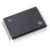
S1D13706F00A200 Epson, S1D13706F00A200 Datasheet - Page 90

S1D13706F00A200
Manufacturer Part Number
S1D13706F00A200
Description
LCD Drivers (QVGA) 320x240 LCD Controller @ 8bpp
Manufacturer
Epson
Datasheet
1.S1D13706F00A200.pdf
(150 pages)
Specifications of S1D13706F00A200
Maximum Clock Frequency
33 MHz
Operating Supply Voltage
1.8 V to 2.2 V, 3 V to 3.6 V
Maximum Operating Temperature
+ 85 C
Package / Case
TQFP-100
Attached Touch Screen
No
Minimum Operating Temperature
- 40 C
Lead Free Status / RoHS Status
Lead free / RoHS Compliant
Available stocks
Company
Part Number
Manufacturer
Quantity
Price
Company:
Part Number:
S1D13706F00A200
Manufacturer:
Epson Electronics America Inc-Semiconductor Div
Quantity:
10 000
- Current page: 90 of 150
- Download datasheet (4Mb)
REG[7Ch] PIP
REG[7Eh] PIP
REG[81h] PIP
REG[85h] PIP
REG[89h] PIP
REG[8Dh] PIP
REG[91h] PIP
REG[A0h] Power Save Configuration Register
REG[A2h] Reserved
REG[A4h] Scratch Pad Register 0
REG[A8h] General Purpose IO Pins Configuration Register 0
REG[ACh] General Purpose IO Pins Status/Control Register 0 120
REG[B0h] PWM Clock / CV Pulse Control Register
REG[B2h] CV Pulse Burst Length Register
Page 90
S1D13706
X31B-A-001-10
+
+
+
+
+
+
+
Window Line Address Offset Register 1
Window X Start Position Register 1
Window Y Start Position Register 1
Window Y End Position Register 1
Window Display Start Address Register 0
Window Display Start Address Register 2
Window X End Position Register 1
Register
PWM Clock and CV Pulse Configuration Registers
Picture-in-Picture Plus (PIP
Table 8-1: S1D13706 Register Set
General Purpose IO Pins Registers
Miscellaneous Registers
111
111
112
113
114
115
116
117
118
118
119
123
126
Pg
Revision 10.3
REG[7Dh] PIP
REG[80h] PIP
REG[84h] PIP
REG[88h] PIP
REG[8Ch] PIP
REG[90h] PIP
REG[A1h] Reserved
REG[A3h] Reserved
REG[A5h] Scratch Pad Register 1
REG[A9h] General Purpose IO Pins Configuration Register 1
REG[ADh] General Purpose IO Pins Status/Control Register 1 122
REG[B1h] PWM Clock / CV Pulse Configuration Register
REG[B3h] PWMOUT Duty Cycle Register
+
) Registers
+
+
+
+
+
+
Window Line Address Offset Register 0
Window X Start Position Register 0
Window Y Start Position Register 0
Window Y End Position Register 0
Window Display Start Address Register 1
Window X End Position Register 0
Register
Epson Research and Development
Hardware Functional Specification
Vancouver Design Center
Issue Date: 2008/12/16
111
112
113
114
115
116
117
118
118
119
125
126
Pg
Related parts for S1D13706F00A200
Image
Part Number
Description
Manufacturer
Datasheet
Request
R

Part Number:
Description:
Display Modules & Development Tools S1D13706F00A Evaluation Board
Manufacturer:
Epson

Part Number:
Description:
INK CARTRIDGE, T0803, EPSON, MAG
Manufacturer:
Epson
Datasheet:

Part Number:
Description:
CXA1034M
Manufacturer:
EPSON Electronics
Datasheet:

Part Number:
Description:
Manufacturer:
EPSON Electronics
Datasheet:

Part Number:
Description:
Manufacturer:
EPSON Electronics
Datasheet:

Part Number:
Description:
Manufacturer:
EPSON Electronics
Datasheet:

Part Number:
Description:
Manufacturer:
EPSON Electronics
Datasheet:

Part Number:
Description:
RTC58321Real time clock module(4-bit I/O CONNECTION REAL TIME CLOCK MODULE)
Manufacturer:
EPSON Electronics
Datasheet:

Part Number:
Description:
SCI7661DC-DC Converter
Manufacturer:
EPSON Electronics
Datasheet:

Part Number:
Description:
Manufacturer:
EPSON Electronics
Datasheet:

Part Number:
Description:
Manufacturer:
EPSON Electronics
Datasheet:


