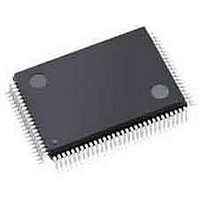
S1D13706F00A200 Epson, S1D13706F00A200 Datasheet - Page 117

S1D13706F00A200
Manufacturer Part Number
S1D13706F00A200
Description
LCD Drivers (QVGA) 320x240 LCD Controller @ 8bpp
Manufacturer
Epson
Datasheet
1.S1D13706F00A200.pdf
(150 pages)
Specifications of S1D13706F00A200
Maximum Clock Frequency
33 MHz
Operating Supply Voltage
1.8 V to 2.2 V, 3 V to 3.6 V
Maximum Operating Temperature
+ 85 C
Package / Case
TQFP-100
Attached Touch Screen
No
Minimum Operating Temperature
- 40 C
Lead Free Status / RoHS Status
Lead free / RoHS Compliant
Available stocks
Company
Part Number
Manufacturer
Quantity
Price
Company:
Part Number:
S1D13706F00A200
Manufacturer:
Epson Electronics America Inc-Semiconductor Div
Quantity:
10 000
- Current page: 117 of 150
- Download datasheet (4Mb)
Epson Research and Development
Vancouver Design Center
8.3.7 Miscellaneous Registers
bit 7
bit 3
bit 0
bit 0
Hardware Functional Specification
Issue Date: 2008/12/16
Power Save Configuration Register
REG[A0h]
Reserved
REG[A1h]
Period Status
Vertical Non-
Display
(RO)
7
7
6
6
Note
Note
Vertical Non-Display Period Status
This is a read-only status bit.
When this bit = 0, the LCD panel output is in a Vertical Display Period.
When this bit = 1, the LCD panel output is in a Vertical Non-Display Period.
Memory Controller Power Save Status
This read-only status bit indicates the power save state of the memory controller.
When this bit = 0, the memory controller is powered up.
When this bit = 1, the memory controller is powered down and the MCLK source can be
turned off.
Power Save Mode Enable
When this bit = 1, the software initiated power save mode is enabled.
When this bit = 0, the software initiated power save mode is disabled.
At reset, this bit is set to 1. For a summary of Power Save Mode, see Section 15, “Power
Save Mode” on page 146.
Reserved.
This bit must remain at 0.
Memory writes are possible during power save mode because the S1D13706 dynamical-
ly enables the memory controller for display buffer writes.
Memory writes are possible during power save mode because the S1D13706 dynamical-
ly enables the memory controller for display buffer writes.
n/a
5
5
n/a
4
4
Revision 10.3
Power Save
Status (RO)
Controller
Memory
3
3
2
2
n/a
1
1
Read/Write
Read/Write
Mode Enable
Power Save
X31B-A-001-10
Reserved
S1D13706
0
0
Page 117
Related parts for S1D13706F00A200
Image
Part Number
Description
Manufacturer
Datasheet
Request
R

Part Number:
Description:
Display Modules & Development Tools S1D13706F00A Evaluation Board
Manufacturer:
Epson

Part Number:
Description:
INK CARTRIDGE, T0803, EPSON, MAG
Manufacturer:
Epson
Datasheet:

Part Number:
Description:
CXA1034M
Manufacturer:
EPSON Electronics
Datasheet:

Part Number:
Description:
Manufacturer:
EPSON Electronics
Datasheet:

Part Number:
Description:
Manufacturer:
EPSON Electronics
Datasheet:

Part Number:
Description:
Manufacturer:
EPSON Electronics
Datasheet:

Part Number:
Description:
Manufacturer:
EPSON Electronics
Datasheet:

Part Number:
Description:
RTC58321Real time clock module(4-bit I/O CONNECTION REAL TIME CLOCK MODULE)
Manufacturer:
EPSON Electronics
Datasheet:

Part Number:
Description:
SCI7661DC-DC Converter
Manufacturer:
EPSON Electronics
Datasheet:

Part Number:
Description:
Manufacturer:
EPSON Electronics
Datasheet:

Part Number:
Description:
Manufacturer:
EPSON Electronics
Datasheet:


