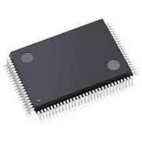
S1D13706F00A200 Epson, S1D13706F00A200 Datasheet - Page 35

S1D13706F00A200
Manufacturer Part Number
S1D13706F00A200
Description
LCD Drivers (QVGA) 320x240 LCD Controller @ 8bpp
Manufacturer
Epson
Datasheet
1.S1D13706F00A200.pdf
(150 pages)
Specifications of S1D13706F00A200
Maximum Clock Frequency
33 MHz
Operating Supply Voltage
1.8 V to 2.2 V, 3 V to 3.6 V
Maximum Operating Temperature
+ 85 C
Package / Case
TQFP-100
Attached Touch Screen
No
Minimum Operating Temperature
- 40 C
Lead Free Status / RoHS Status
Lead free / RoHS Compliant
Available stocks
Company
Part Number
Manufacturer
Quantity
Price
Company:
Part Number:
S1D13706F00A200
Manufacturer:
Epson Electronics America Inc-Semiconductor Div
Quantity:
10 000
- Current page: 35 of 150
- Download datasheet (4Mb)
Epson Research and Development
Vancouver Design Center
1. t11 is the delay from when data is placed on the bus until the data is latched into the write buffer.
2. When
3. When
4. When
5. When
Hardware Functional Specification
Issue Date: 2008/12/16
T
Symbol
f
BUSCLK
BUSCLK
t7a
t7b
t7c
t7d
t10
t11
t12
t13
t14
t15
t1
t2
t3
t4
t5
t6
t8
t9
Bus Clock frequency
Bus Clock period
Clock pulse width high
Clock pulse width low
SA[16:0], M/R#, SBHE# setup to first BUSCLK rising edge
where CS# = 0 and either MEMR# = 0 or MEMW# = 0
SA[16:0], M/R#, SBHE# hold from either MEMR# or MEMW#
rising edge
CS# setup to BUSCLK rising edge
CS# hold from either MEMR# or MEMW# rising edge
MEMR#/MEMW# asserted for MCLK = BCLK when IOCHRDY
is not used (see Note 2)
MEMR#/MEMW# asserted for MCLK = BCLK ÷ 2 when
IOCHRDY is not used (see Note 3)
MEMR#/MEMW# asserted for MCLK = BCLK ÷ 3 when
IOCHRDY is not used (see Note 4)
MEMR#/MEMW# asserted for MCLK = BCLK ÷ 4 when
IOCHRDY is not used (see Note 5)
MEMR# or MEMW# setup to BUSCLK rising edge
Falling edge of either MEMR# or MEMW# to IOCHRDY driven
low
Rising edge of either MEMR# or MEMW# to IOCHRDY high
impedance
SD[15:0] setup to third BUSCLK rising edge where CS# = 0 and
MEMW# = 0 (write cycle) (see note 1)
SD[15:0] hold from IOCHRDY rising edge (write cycle)
MEMR# falling edge to SD[15:0] driven (read cycle)
IOCHRDY rising edge to SD[15:0] valid (read cycle)
Rising edge of MEMR# to SD[15:0] high impedance (read
cycle)
IOCHRDY
IOCHRDY
IOCHRDY
IOCHRDY
is used, the Host will assert MEMR#/MEMW# for up to 8.5T
is used, the Host will assert MEMR#/MEMW# for up to 11.5T
is used, the Host will assert MEMR#/MEMW# for up to 13.5T
is used, the Host will assert MEMR#/MEMW# for up to 17.5T
Parameter
Table 6-6: Generic #2 Interface Timing
Revision 10.3
1/f
BUSCLK
22.5
22.5
11.5
13.5
17.5
Min
8.5
1
0
0
0
2
5
5
1
1
4
5
2.0V
Max
BUSCLK
20
26
33
0
BUSCLK
BUSCLK
BUSCLK
1/f
.
.
.
.
BUSCLK
Min
11
13
17
9
9
1
0
1
0
8
1
3
3
0
0
3
3
3.3V
Max
50
15
13
13
12
2
X31B-A-001-10
S1D13706
T
T
T
T
BUSCLK
BUSCLK
BUSCLK
BUSCLK
Page 35
Unit
MHz
ns
ns
ns
ns
ns
ns
ns
ns
ns
ns
ns
ns
ns
ns
ns
Related parts for S1D13706F00A200
Image
Part Number
Description
Manufacturer
Datasheet
Request
R

Part Number:
Description:
Display Modules & Development Tools S1D13706F00A Evaluation Board
Manufacturer:
Epson

Part Number:
Description:
INK CARTRIDGE, T0803, EPSON, MAG
Manufacturer:
Epson
Datasheet:

Part Number:
Description:
CXA1034M
Manufacturer:
EPSON Electronics
Datasheet:

Part Number:
Description:
Manufacturer:
EPSON Electronics
Datasheet:

Part Number:
Description:
Manufacturer:
EPSON Electronics
Datasheet:

Part Number:
Description:
Manufacturer:
EPSON Electronics
Datasheet:

Part Number:
Description:
Manufacturer:
EPSON Electronics
Datasheet:

Part Number:
Description:
RTC58321Real time clock module(4-bit I/O CONNECTION REAL TIME CLOCK MODULE)
Manufacturer:
EPSON Electronics
Datasheet:

Part Number:
Description:
SCI7661DC-DC Converter
Manufacturer:
EPSON Electronics
Datasheet:

Part Number:
Description:
Manufacturer:
EPSON Electronics
Datasheet:

Part Number:
Description:
Manufacturer:
EPSON Electronics
Datasheet:


