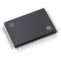
S1D13706F00A200 Epson, S1D13706F00A200 Datasheet - Page 144

S1D13706F00A200
Manufacturer Part Number
S1D13706F00A200
Description
LCD Drivers (QVGA) 320x240 LCD Controller @ 8bpp
Manufacturer
Epson
Datasheet
1.S1D13706F00A200.pdf
(150 pages)
Specifications of S1D13706F00A200
Maximum Clock Frequency
33 MHz
Operating Supply Voltage
1.8 V to 2.2 V, 3 V to 3.6 V
Maximum Operating Temperature
+ 85 C
Package / Case
TQFP-100
Attached Touch Screen
No
Minimum Operating Temperature
- 40 C
Lead Free Status / RoHS Status
Lead free / RoHS Compliant
Available stocks
Company
Part Number
Manufacturer
Quantity
Price
Company:
Part Number:
S1D13706F00A200
Manufacturer:
Epson Electronics America Inc-Semiconductor Div
Quantity:
10 000
- Current page: 144 of 150
- Download datasheet (4Mb)
Page 144
14.1.1 16 Bpp Color Depth
S1D13706
X31B-A-001-10
System
Memory
Address
* MSB is assumed to be associated with even address.
* LSB is assumed to be associated with odd address.
15
0
2
MSB
aa
cc
LSB
bb
dd
For 16 bpp color depth, the Display Data Byte Swap bit (REG[71h] bit 6) must be set
to 1.
For 16 bpp color depth, the MSB of the 16-bit pixel data is stored at the even system
memory address location and the LSB of the 16-bit pixel data is stored at the odd system
memory address location. Bus data byte swapping (automatic when the S1D13706 is
configured for Big-Endian) causes the 16-bit pixel data to be stored byte-swapped in the
S1D13706 display buffer. During display refresh this stored data must be byte-swapped
again before it is sent to the display.
0
System
Memory
(Big-Endian)
D[15:8]
D[7:0]
Figure 14-1: Byte-swapping for 16 Bpp
CPU Data
Byte Swap
Display
Buffer
(Little-Endian)
Revision 10.3
15
bb
dd
cc
aa
0
0
2
Byte Swap
Display
Data
Display
Buffer
Address
aabb ccdd
Epson Research and Development
Hardware Functional Specification
Vancouver Design Center
Issue Date: 2008/12/16
Related parts for S1D13706F00A200
Image
Part Number
Description
Manufacturer
Datasheet
Request
R

Part Number:
Description:
Display Modules & Development Tools S1D13706F00A Evaluation Board
Manufacturer:
Epson

Part Number:
Description:
INK CARTRIDGE, T0803, EPSON, MAG
Manufacturer:
Epson
Datasheet:

Part Number:
Description:
CXA1034M
Manufacturer:
EPSON Electronics
Datasheet:

Part Number:
Description:
Manufacturer:
EPSON Electronics
Datasheet:

Part Number:
Description:
Manufacturer:
EPSON Electronics
Datasheet:

Part Number:
Description:
Manufacturer:
EPSON Electronics
Datasheet:

Part Number:
Description:
Manufacturer:
EPSON Electronics
Datasheet:

Part Number:
Description:
RTC58321Real time clock module(4-bit I/O CONNECTION REAL TIME CLOCK MODULE)
Manufacturer:
EPSON Electronics
Datasheet:

Part Number:
Description:
SCI7661DC-DC Converter
Manufacturer:
EPSON Electronics
Datasheet:

Part Number:
Description:
Manufacturer:
EPSON Electronics
Datasheet:

Part Number:
Description:
Manufacturer:
EPSON Electronics
Datasheet:


