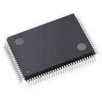
S1D13706F00A200 Epson, S1D13706F00A200 Datasheet - Page 101

S1D13706F00A200
Manufacturer Part Number
S1D13706F00A200
Description
LCD Drivers (QVGA) 320x240 LCD Controller @ 8bpp
Manufacturer
Epson
Datasheet
1.S1D13706F00A200.pdf
(150 pages)
Specifications of S1D13706F00A200
Maximum Clock Frequency
33 MHz
Operating Supply Voltage
1.8 V to 2.2 V, 3 V to 3.6 V
Maximum Operating Temperature
+ 85 C
Package / Case
TQFP-100
Attached Touch Screen
No
Minimum Operating Temperature
- 40 C
Lead Free Status / RoHS Status
Lead free / RoHS Compliant
Available stocks
Company
Part Number
Manufacturer
Quantity
Price
Company:
Part Number:
S1D13706F00A200
Manufacturer:
Epson Electronics America Inc-Semiconductor Div
Quantity:
10 000
- Current page: 101 of 150
- Download datasheet (4Mb)
Epson Research and Development
Vancouver Design Center
bits 9-0
bit 7
bits 6-0
Hardware Functional Specification
Issue Date: 2008/12/16
Vertical Display Period Start Position Register 0
REG[1Eh]
Vertical Display Period Start Position Register 1
REG[1Fh]
FPLINE Pulse Width Register
REG[20h]
FPLINE Pulse
Polarity
7
7
7
6
6
6
Note
Note
Vertical Display Period Start Position Bits [9:0]
These bits specify the Vertical Display Period Start Position for panels in 1 line resolution.
For passive LCD panels these bits must be set to 00h.
For TFT panels, VDPS is calculated using the following formula.
FPLINE Pulse Polarity
This bit selects the polarity of the horizontal sync signal. For passive panels, this bit must
be set to 1. For TFT panels, this bit is set according to the horizontal sync signal of the
panel (typically FPLINE or LP).
When this bit = 0, the horizontal sync signal is active low.
When this bit = 1, the horizontal sync signal is active high.
FPLINE Pulse Width Bits [6:0]
These bits specify the width of the panel horizontal sync signal, in 1 pixel resolution. The
horizontal sync signal is typically FPLINE or LP, depending on the panel type.
FPLINE Pulse Width in number of pixels = (REG[20h] bits 6:0) + 1
1
2
face” on page 52.
For panel AC timing and timing parameter definitions, see Section 6.4, “Display Inter-
face” on page 52.
For panel AC timing and timing parameter definitions, see Section 6.4, “Display Inter-
This register must be programmed such that the following formula is valid.
VDPS + VDP < VT
VDPS = (REG[1Fh] bits 1-0, REG[1Eh] bits 7-0)
5
5
5
Vertical Display Period Start Position Bits 7-0
n/a
4
4
4
FPLINE Pulse Width Bits 6-0
Revision 10.3
3
3
3
2
2
2
Vertical Display Period Start
1
1
1
Position Bits 9-8
Read/Write
Read/Write
Read/Write
X31B-A-001-10
S1D13706
0
0
0
Page 101
Related parts for S1D13706F00A200
Image
Part Number
Description
Manufacturer
Datasheet
Request
R

Part Number:
Description:
Display Modules & Development Tools S1D13706F00A Evaluation Board
Manufacturer:
Epson

Part Number:
Description:
INK CARTRIDGE, T0803, EPSON, MAG
Manufacturer:
Epson
Datasheet:

Part Number:
Description:
CXA1034M
Manufacturer:
EPSON Electronics
Datasheet:

Part Number:
Description:
Manufacturer:
EPSON Electronics
Datasheet:

Part Number:
Description:
Manufacturer:
EPSON Electronics
Datasheet:

Part Number:
Description:
Manufacturer:
EPSON Electronics
Datasheet:

Part Number:
Description:
Manufacturer:
EPSON Electronics
Datasheet:

Part Number:
Description:
RTC58321Real time clock module(4-bit I/O CONNECTION REAL TIME CLOCK MODULE)
Manufacturer:
EPSON Electronics
Datasheet:

Part Number:
Description:
SCI7661DC-DC Converter
Manufacturer:
EPSON Electronics
Datasheet:

Part Number:
Description:
Manufacturer:
EPSON Electronics
Datasheet:

Part Number:
Description:
Manufacturer:
EPSON Electronics
Datasheet:


