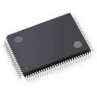
S1D13706F00A200 Epson, S1D13706F00A200 Datasheet - Page 89

S1D13706F00A200
Manufacturer Part Number
S1D13706F00A200
Description
LCD Drivers (QVGA) 320x240 LCD Controller @ 8bpp
Manufacturer
Epson
Datasheet
1.S1D13706F00A200.pdf
(150 pages)
Specifications of S1D13706F00A200
Maximum Clock Frequency
33 MHz
Operating Supply Voltage
1.8 V to 2.2 V, 3 V to 3.6 V
Maximum Operating Temperature
+ 85 C
Package / Case
TQFP-100
Attached Touch Screen
No
Minimum Operating Temperature
- 40 C
Lead Free Status / RoHS Status
Lead free / RoHS Compliant
Available stocks
Company
Part Number
Manufacturer
Quantity
Price
Company:
Part Number:
S1D13706F00A200
Manufacturer:
Epson Electronics America Inc-Semiconductor Div
Quantity:
10 000
- Current page: 89 of 150
- Download datasheet (4Mb)
REG[00h] Revision Code Register
REG[02h] Configuration Readback Register
REG[04h] Memory Clock Configuration Register
REG[08h] Look-Up Table Blue Write Data Register
REG[0Ah] Look-Up Table Red Write Data Register
REG[0Ch] Look-Up Table Blue Read Data Register
REG[0Eh] Look-Up Table Red Read Data Register
REG[10h] Panel Type Register
REG[12h] Horizontal Total Register
REG[16h] Horizontal Display Period Start Position Register 0
REG[18h] Vertical Total Register 0
REG[1Ch] Vertical Display Period Register 0
REG[1Eh] Vertical Display Period Start Position Register 0
REG[20h] FPLINE Pulse Width Register
REG[23h] FPLINE Pulse Start Position Register 1
REG[26h] FPFRAME Pulse Start Position Register 0
REG[28h] D-TFD GCP Index Register
REG[70h] Display Mode Register
REG[74h] Main Window Display Start Address Register 0
REG[76h] Main Window Display Start Address Register 2
REG[79h] Main Window Line Address Offset Register 1
Epson Research and Development
Vancouver Design Center
8 Registers
8.1 Register Mapping
8.2 Register Set
Hardware Functional Specification
Issue Date: 2008/12/16
Register
This section discusses how and where to access the S1D13706 registers. It also provides
detailed information about the layout and usage of each register.
The S1D13706 registers are memory-mapped. When the system decodes the input pins as
CS# = 0 and M/R# = 0, the registers may be accessed. The register space is decoded by
A[16:0].
The S1D13706 register set is as follows.
Table 8-1: S1D13706 Register Set
Read-Only Configuration Registers
Clock Configuration Registers
Panel Configuration Registers
Look-Up Table Registers
Display Mode Registers
100
100
101
101
102
103
103
105
109
109
110
Pg
Revision 10.3
91
91
92
94
95
95
96
97
98
99
REG[01h] Display Buffer Size Register
REG[09h] Look-Up Table Green Write Data Register
REG[0Bh] Look-Up Table Write Address Register
REG[0Fh] Look-Up Table Read Address Register
REG[14h] Horizontal Display Period Register
REG[17h] Horizontal Display Period Start Position Register 1
REG[1Dh] Vertical Display Period Register 1
REG[1Fh] Vertical Display Period Start Position Register 1
REG[27h] FPFRAME Pulse Start Position Register 1
REG[2Ch] D-TFD GCP Data Register
REG[71h] Special Effects Register
REG[75h] Main Window Display Start Address Register 1
REG[78h] Main Window Line Address Offset Register 0
REG[05h] Pixel Clock Configuration Register
REG[0Dh] Look-Up Table Green Read Data Register
REG[11h] MOD Rate Register
REG[19h] Vertical Total Register 1
REG[22h] FPLINE Pulse Start Position Register 0
REG[24h] FPFRAME Pulse Width Register
Register
X31B-A-001-10
S1D13706
Page 89
100
100
101
102
103
104
107
109
110
102
Pg
91
93
94
95
96
96
98
99
99
Related parts for S1D13706F00A200
Image
Part Number
Description
Manufacturer
Datasheet
Request
R

Part Number:
Description:
Display Modules & Development Tools S1D13706F00A Evaluation Board
Manufacturer:
Epson

Part Number:
Description:
INK CARTRIDGE, T0803, EPSON, MAG
Manufacturer:
Epson
Datasheet:

Part Number:
Description:
CXA1034M
Manufacturer:
EPSON Electronics
Datasheet:

Part Number:
Description:
Manufacturer:
EPSON Electronics
Datasheet:

Part Number:
Description:
Manufacturer:
EPSON Electronics
Datasheet:

Part Number:
Description:
Manufacturer:
EPSON Electronics
Datasheet:

Part Number:
Description:
Manufacturer:
EPSON Electronics
Datasheet:

Part Number:
Description:
RTC58321Real time clock module(4-bit I/O CONNECTION REAL TIME CLOCK MODULE)
Manufacturer:
EPSON Electronics
Datasheet:

Part Number:
Description:
SCI7661DC-DC Converter
Manufacturer:
EPSON Electronics
Datasheet:

Part Number:
Description:
Manufacturer:
EPSON Electronics
Datasheet:

Part Number:
Description:
Manufacturer:
EPSON Electronics
Datasheet:


