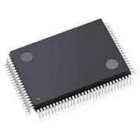
S1D13706F00A200 Epson, S1D13706F00A200 Datasheet - Page 20

S1D13706F00A200
Manufacturer Part Number
S1D13706F00A200
Description
LCD Drivers (QVGA) 320x240 LCD Controller @ 8bpp
Manufacturer
Epson
Datasheet
1.S1D13706F00A200.pdf
(150 pages)
Specifications of S1D13706F00A200
Maximum Clock Frequency
33 MHz
Operating Supply Voltage
1.8 V to 2.2 V, 3 V to 3.6 V
Maximum Operating Temperature
+ 85 C
Package / Case
TQFP-100
Attached Touch Screen
No
Minimum Operating Temperature
- 40 C
Lead Free Status / RoHS Status
Lead free / RoHS Compliant
Available stocks
Company
Part Number
Manufacturer
Quantity
Price
Company:
Part Number:
S1D13706F00A200
Manufacturer:
Epson Electronics America Inc-Semiconductor Div
Quantity:
10 000
- Current page: 20 of 150
- Download datasheet (4Mb)
Page 20
S1D13706
X31B-A-001-10
Pin Name Type Pin #
RD/WR#
RD#
BS#
I
I
I
12
8
9
Cell
LIS
LIS
LIS
HIOVDD
HIOVDD
HIOVDD
Table 4-2: Host Interface Pin Descriptions
Voltage
IO
RESET#
State
—
—
—
Revision 10.3
This input pin has multiple functions.
See Table 4-8: “Host Bus Interface Pin Mapping,” on page 26 for
summary.
This input pin has multiple functions.
See Table 4-8: “Host Bus Interface Pin Mapping,” on page 26 for
summary.
This input pin has multiple functions.
See Table 4-8: “Host Bus Interface Pin Mapping,” on page 26 for
summary.
• For Generic #1, this pin must be tied to HIO V
• For Generic #2, this pin must be tied to HIO V
• For SH-3/SH-4, this pin inputs the bus start signal (BS#).
• For MC68K #1, this pin inputs the address strobe (AS#).
• For MC68K #2, this pin inputs the address strobe (AS#).
• For REDCAP2, this pin must be tied to HIO V
• For DragonBall, this pin must be tied to HIO V
• For Generic #1, this pin inputs the read command for the
• For Generic #2, this pin must be tied to HIO V
• For SH-3/SH-4, this pin inputs the RD/WR# signal. The
• For MC68K #1, this pin inputs the R/W# signal.
• For MC68K #2, this pin inputs the R/W# signal.
• For REDCAP2, this pin inputs the R/W signal.
• For DragonBall, this pin must be tied to HIO V
• For Generic #1, this pin inputs the read command for the lower
• For Generic #2, this pin inputs the read command (RD#).
• For SH-3/SH-4, this pin inputs the read signal (RD#).
• For MC68K #1, this pin must be tied to HIO V
• For MC68K #2, this pin inputs the bus size bit 1 (SIZ1).
• For REDCAP2, this pin inputs the output enable (OE).
• For DragonBall, this pin inputs the output enable (OE).
upper data byte (RD1#).
S1D13706 needs this signal for early decode of the bus cycle.
data byte (RD0#).
Description
Epson Research and Development
Hardware Functional Specification
Vancouver Design Center
Issue Date: 2008/12/16
DD
DD
DD
DD
DD
DD
DD
.
.
.
.
.
.
.
Related parts for S1D13706F00A200
Image
Part Number
Description
Manufacturer
Datasheet
Request
R

Part Number:
Description:
Display Modules & Development Tools S1D13706F00A Evaluation Board
Manufacturer:
Epson

Part Number:
Description:
INK CARTRIDGE, T0803, EPSON, MAG
Manufacturer:
Epson
Datasheet:

Part Number:
Description:
CXA1034M
Manufacturer:
EPSON Electronics
Datasheet:

Part Number:
Description:
Manufacturer:
EPSON Electronics
Datasheet:

Part Number:
Description:
Manufacturer:
EPSON Electronics
Datasheet:

Part Number:
Description:
Manufacturer:
EPSON Electronics
Datasheet:

Part Number:
Description:
Manufacturer:
EPSON Electronics
Datasheet:

Part Number:
Description:
RTC58321Real time clock module(4-bit I/O CONNECTION REAL TIME CLOCK MODULE)
Manufacturer:
EPSON Electronics
Datasheet:

Part Number:
Description:
SCI7661DC-DC Converter
Manufacturer:
EPSON Electronics
Datasheet:

Part Number:
Description:
Manufacturer:
EPSON Electronics
Datasheet:

Part Number:
Description:
Manufacturer:
EPSON Electronics
Datasheet:


