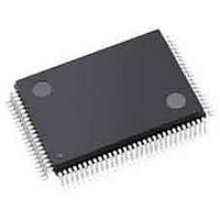
S1D13706F00A200 Epson, S1D13706F00A200 Datasheet - Page 84

S1D13706F00A200
Manufacturer Part Number
S1D13706F00A200
Description
LCD Drivers (QVGA) 320x240 LCD Controller @ 8bpp
Manufacturer
Epson
Datasheet
1.S1D13706F00A200.pdf
(150 pages)
Specifications of S1D13706F00A200
Maximum Clock Frequency
33 MHz
Operating Supply Voltage
1.8 V to 2.2 V, 3 V to 3.6 V
Maximum Operating Temperature
+ 85 C
Package / Case
TQFP-100
Attached Touch Screen
No
Minimum Operating Temperature
- 40 C
Lead Free Status / RoHS Status
Lead free / RoHS Compliant
Available stocks
Company
Part Number
Manufacturer
Quantity
Price
Company:
Part Number:
S1D13706F00A200
Manufacturer:
Epson Electronics America Inc-Semiconductor Div
Quantity:
10 000
- Current page: 84 of 150
- Download datasheet (4Mb)
Page 84
7 Clocks
7.1 Clock Descriptions
7.1.1 BCLK
7.1.2 MCLK
S1D13706
X31B-A-001-10
Note
Note
BCLK is an internal clock derived from CLKI. BCLK can be a divided version (÷1, ÷2, ÷3,
÷4) of CLKI. CLKI is typically derived from the host CPU bus clock.
The source clock options for BCLK may be selected as in the following table.
MCLK provides the internal clock required to access the embedded SRAM. The S1D13706
is designed with efficient power saving control for clocks (clocks are turned off when not
used); reducing the frequency of MCLK does not necessarily save more power.
Furthermore, reducing the MCLK frequency relative to the BCLK frequency increases the
CPU cycle latency and so reduces screen update performance. For a balance of power
saving and performance, the MCLK should be configured to have a high enough frequency
setting to provide sufficient screen refresh as well as acceptable CPU cycle latency.
The source clock options for MCLK may be selected as in the following table.
For synchronous bus interfaces, it is recommended that BCLK be set the same as the
CPU bus clock (not a divided version of CLKI) e.g. SH-3, SH-4.
The CLKI ÷ 3 and CLKI ÷ 4 options may not work properly with bus interfaces with
short back-to-back cycle timing.
Source Clock Options
Source Clock Options
Revision 10.3
BCLK
BCLK
BCLK
CLKI
CLKI
CLKI
Table 7-2: MCLK Clock Selection
Table 7-1: BCLK Clock Selection
BCLK
CLKI
÷
÷
÷
÷
÷
÷
2
3
4
2
3
4
REG[04h] bit 5,4 = 00
REG[04h] bit 5,4 = 01
REG[04h] bit 5,4 = 10
REG[04h] bit 5,4 = 11
BCLK Selection
MCLK Selection
CNF[7:6] = 00
CNF[7:6] = 01
CNF[7:6] = 10
CNF[7:6] = 11
Epson Research and Development
Hardware Functional Specification
Vancouver Design Center
Issue Date: 2008/12/16
Related parts for S1D13706F00A200
Image
Part Number
Description
Manufacturer
Datasheet
Request
R

Part Number:
Description:
Display Modules & Development Tools S1D13706F00A Evaluation Board
Manufacturer:
Epson

Part Number:
Description:
INK CARTRIDGE, T0803, EPSON, MAG
Manufacturer:
Epson
Datasheet:

Part Number:
Description:
CXA1034M
Manufacturer:
EPSON Electronics
Datasheet:

Part Number:
Description:
Manufacturer:
EPSON Electronics
Datasheet:

Part Number:
Description:
Manufacturer:
EPSON Electronics
Datasheet:

Part Number:
Description:
Manufacturer:
EPSON Electronics
Datasheet:

Part Number:
Description:
Manufacturer:
EPSON Electronics
Datasheet:

Part Number:
Description:
RTC58321Real time clock module(4-bit I/O CONNECTION REAL TIME CLOCK MODULE)
Manufacturer:
EPSON Electronics
Datasheet:

Part Number:
Description:
SCI7661DC-DC Converter
Manufacturer:
EPSON Electronics
Datasheet:

Part Number:
Description:
Manufacturer:
EPSON Electronics
Datasheet:

Part Number:
Description:
Manufacturer:
EPSON Electronics
Datasheet:


