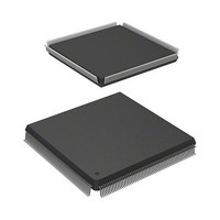
R5S72030W200FP Renesas Electronics America, R5S72030W200FP Datasheet - Page 7

R5S72030W200FP
Manufacturer Part Number
R5S72030W200FP
Description
IC SUPERH MPU ROMLESS 240QFP
Manufacturer
Renesas Electronics America
Series
SuperH® SH7200r
Specifications of R5S72030W200FP
Core Processor
SH2A-FPU
Core Size
32-Bit
Speed
200MHz
Connectivity
CAN, I²C, SCI, SSI, SSU, USB
Peripherals
DMA, LCD, POR, PWM, WDT
Number Of I /o
82
Program Memory Type
ROMless
Ram Size
80K x 8
Voltage - Supply (vcc/vdd)
1.1 V ~ 3.6 V
Data Converters
A/D 8x10b; D/A 2x8b
Oscillator Type
Internal
Operating Temperature
-20°C ~ 85°C
Package / Case
240-QFP
For Use With
R0K572030S000BE - KIT DEV FOR SH7203HS0005KCU11H - EMULATOR E10A-USB H8S(X),SH2(A)
Lead Free Status / RoHS Status
Contains lead / RoHS non-compliant
Eeprom Size
-
Program Memory Size
-
Available stocks
Company
Part Number
Manufacturer
Quantity
Price
Company:
Part Number:
R5S72030W200FP
Manufacturer:
SAMSUNG
Quantity:
1 001
Company:
Part Number:
R5S72030W200FP
Manufacturer:
Renesas Electronics America
Quantity:
10 000
- Current page: 7 of 503
- Download datasheet (3Mb)
Item
6.4.48 RTE
ReTurn from
Exception
System Control
Instruction
6.4.50
SET T bit
System Control
Instruction
6.4.57 SLEEP
SLEEP
System Control
Instruction
6.5.10 FLOAT
Floating-point
convert from integer
Floating-Point
Instruction
7.1 Overview
Figure 7.1 Overview
of Register Bank
Configuration
7.2.1 Banked Data
7.2.2 Register
Banks
7.2.3 Bank Control
Registers
(2) Bank Number
Register (IBNR) (16
bit, Initial value:
H'0000)
7.3.1 Save to Bank 328
Figure 7.2 Bank
Save Operations
Figure 7.3 Bank
Save Timing
SETT
Page
326
244
248
257
296
325
326
327
328,
329
Revision (See Manual for Details)
Description amended
Return from
Exception Handling
Description amended
T Bit Setting
Description amended
Transition to Power-Down Mode
Description amended
⋅⋅⋅ When FPSCR.enable.I = 1, and FPSCR.PR = 0, an FPU
exception trap is generated regardless of whether or not an
exception has occurred.⋅⋅⋅
Figure amended
(Before) IVO → (After) VTO
Figure notes amended
VTO: Interrupt vector table address offset
Description amended
⋅⋅⋅ and the interrupt vector table address offsets (VTO) are banked.
Description amended
⋅⋅⋅ Register banks are stacked in first in last out (FILO) sequence.⋅⋅⋅
Description amended
Bits 3 to 0: BN3 to BN0
⋅⋅⋅ after which the data is retrieved from the register bank. These
bits are read-only and cannot be modified.
Description amended
(b) ..., and the interrupt vector table address offset (VTO) are
saved to the bank indicated by the BN, bank i.
Figure amended
(Before) IVN → (After) VTO
Delayed Branch Instruction
Rev. 3.00 Jul 08, 2005 page v of xiv
.
Related parts for R5S72030W200FP
Image
Part Number
Description
Manufacturer
Datasheet
Request
R

Part Number:
Description:
KIT STARTER FOR M16C/29
Manufacturer:
Renesas Electronics America
Datasheet:

Part Number:
Description:
KIT STARTER FOR R8C/2D
Manufacturer:
Renesas Electronics America
Datasheet:

Part Number:
Description:
R0K33062P STARTER KIT
Manufacturer:
Renesas Electronics America
Datasheet:

Part Number:
Description:
KIT STARTER FOR R8C/23 E8A
Manufacturer:
Renesas Electronics America
Datasheet:

Part Number:
Description:
KIT STARTER FOR R8C/25
Manufacturer:
Renesas Electronics America
Datasheet:

Part Number:
Description:
KIT STARTER H8S2456 SHARPE DSPLY
Manufacturer:
Renesas Electronics America
Datasheet:

Part Number:
Description:
KIT STARTER FOR R8C38C
Manufacturer:
Renesas Electronics America
Datasheet:

Part Number:
Description:
KIT STARTER FOR R8C35C
Manufacturer:
Renesas Electronics America
Datasheet:

Part Number:
Description:
KIT STARTER FOR R8CL3AC+LCD APPS
Manufacturer:
Renesas Electronics America
Datasheet:

Part Number:
Description:
KIT STARTER FOR RX610
Manufacturer:
Renesas Electronics America
Datasheet:

Part Number:
Description:
KIT STARTER FOR R32C/118
Manufacturer:
Renesas Electronics America
Datasheet:

Part Number:
Description:
KIT DEV RSK-R8C/26-29
Manufacturer:
Renesas Electronics America
Datasheet:

Part Number:
Description:
KIT STARTER FOR SH7124
Manufacturer:
Renesas Electronics America
Datasheet:

Part Number:
Description:
KIT STARTER FOR H8SX/1622
Manufacturer:
Renesas Electronics America
Datasheet:

Part Number:
Description:
KIT DEV FOR SH7203
Manufacturer:
Renesas Electronics America
Datasheet:


