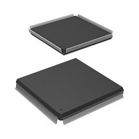
R5S72030W200FP Renesas Electronics America, R5S72030W200FP Datasheet - Page 346

R5S72030W200FP
Manufacturer Part Number
R5S72030W200FP
Description
IC SUPERH MPU ROMLESS 240QFP
Manufacturer
Renesas Electronics America
Series
SuperH® SH7200r
Specifications of R5S72030W200FP
Core Processor
SH2A-FPU
Core Size
32-Bit
Speed
200MHz
Connectivity
CAN, I²C, SCI, SSI, SSU, USB
Peripherals
DMA, LCD, POR, PWM, WDT
Number Of I /o
82
Program Memory Type
ROMless
Ram Size
80K x 8
Voltage - Supply (vcc/vdd)
1.1 V ~ 3.6 V
Data Converters
A/D 8x10b; D/A 2x8b
Oscillator Type
Internal
Operating Temperature
-20°C ~ 85°C
Package / Case
240-QFP
For Use With
R0K572030S000BE - KIT DEV FOR SH7203HS0005KCU11H - EMULATOR E10A-USB H8S(X),SH2(A)
Lead Free Status / RoHS Status
Contains lead / RoHS non-compliant
Eeprom Size
-
Program Memory Size
-
Available stocks
Company
Part Number
Manufacturer
Quantity
Price
Company:
Part Number:
R5S72030W200FP
Manufacturer:
SAMSUNG
Quantity:
1 001
Company:
Part Number:
R5S72030W200FP
Manufacturer:
Renesas Electronics America
Quantity:
10 000
- Current page: 346 of 503
- Download datasheet (3Mb)
Section 7 Register Banks
(2) Retrieve from Stack
If the retrieve from bank instruction, RESBANK, is executed when the register bank overflow bit
in SR is set to 1, the following operations occur.
7.4
The LDBANK and STBANK instructions can be used to send user-defined register bank data to
and from general register R0 for debugging purposes.
7.4.1
(1) LDBANK (Load Data from Register Bank to R0)
Format: LDBANK @Rm,R0
Operation: Sends 4 bytes of data from the register bank address indicated by Rm to R0.
(2) STBANK (Store Data from R0 to Register Bank)
Format: STBANK R0,@Rn
Operation: Sends the contents of R0 to the register bank address indicated by Rn.
7.4.2
Figure 7.4 illustrates the correlation between register bank send command address values (Rm in
the case of LDBANK and Rn in the case of STBANK) and register bank entries. The bank number
is specified by address bits 15 to 7 (BN), and the entry within the bank (R0 to R14, GBR, MACH,
MACL, PR, VTO) is specified by address bits 6 to 2 (EN). Address bits 31 to 16 and 1 to 0 should
all be cleared to 0. If the value of these bits is not all 0 operation cannot be guaranteed in cases
where a nonexistent bank is specified by address bits 15 to 7 or a nonexistent entry is specified by
address bits 6 to 2.
Rev. 3.00 Jul 08, 2005 page 330 of 484
REJ09B0051-0300
(a) The contents of the banked registers (R0 to R14, GBR, MACH, MACL, and PR) are
(b) The bank number (BN) bits in the bank number register (IBNR) remain set to the
retrieved from the stack. The order in which the contents of these registers are retrieved is
R0, R1, … R13, R14, PR, GBR, MACH, MACL.
maximum value, N.
Register Bank Data Send Instructions
Description of Instructions
Register Bank Addressing
Related parts for R5S72030W200FP
Image
Part Number
Description
Manufacturer
Datasheet
Request
R

Part Number:
Description:
KIT STARTER FOR M16C/29
Manufacturer:
Renesas Electronics America
Datasheet:

Part Number:
Description:
KIT STARTER FOR R8C/2D
Manufacturer:
Renesas Electronics America
Datasheet:

Part Number:
Description:
R0K33062P STARTER KIT
Manufacturer:
Renesas Electronics America
Datasheet:

Part Number:
Description:
KIT STARTER FOR R8C/23 E8A
Manufacturer:
Renesas Electronics America
Datasheet:

Part Number:
Description:
KIT STARTER FOR R8C/25
Manufacturer:
Renesas Electronics America
Datasheet:

Part Number:
Description:
KIT STARTER H8S2456 SHARPE DSPLY
Manufacturer:
Renesas Electronics America
Datasheet:

Part Number:
Description:
KIT STARTER FOR R8C38C
Manufacturer:
Renesas Electronics America
Datasheet:

Part Number:
Description:
KIT STARTER FOR R8C35C
Manufacturer:
Renesas Electronics America
Datasheet:

Part Number:
Description:
KIT STARTER FOR R8CL3AC+LCD APPS
Manufacturer:
Renesas Electronics America
Datasheet:

Part Number:
Description:
KIT STARTER FOR RX610
Manufacturer:
Renesas Electronics America
Datasheet:

Part Number:
Description:
KIT STARTER FOR R32C/118
Manufacturer:
Renesas Electronics America
Datasheet:

Part Number:
Description:
KIT DEV RSK-R8C/26-29
Manufacturer:
Renesas Electronics America
Datasheet:

Part Number:
Description:
KIT STARTER FOR SH7124
Manufacturer:
Renesas Electronics America
Datasheet:

Part Number:
Description:
KIT STARTER FOR H8SX/1622
Manufacturer:
Renesas Electronics America
Datasheet:

Part Number:
Description:
KIT DEV FOR SH7203
Manufacturer:
Renesas Electronics America
Datasheet:


