R5S72030W200FP Renesas Electronics America, R5S72030W200FP Datasheet - Page 343
R5S72030W200FP
Manufacturer Part Number
R5S72030W200FP
Description
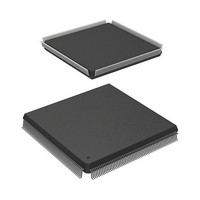
IC SUPERH MPU ROMLESS 240QFP
Manufacturer
Renesas Electronics America
Series
SuperH® SH7200r
Specifications of R5S72030W200FP
Core Processor
SH2A-FPU
Core Size
32-Bit
Speed
200MHz
Connectivity
CAN, I²C, SCI, SSI, SSU, USB
Peripherals
DMA, LCD, POR, PWM, WDT
Number Of I /o
82
Program Memory Type
ROMless
Ram Size
80K x 8
Voltage - Supply (vcc/vdd)
1.1 V ~ 3.6 V
Data Converters
A/D 8x10b; D/A 2x8b
Oscillator Type
Internal
Operating Temperature
-20°C ~ 85°C
Package / Case
240-QFP
For Use With
R0K572030S000BE - KIT DEV FOR SH7203HS0005KCU11H - EMULATOR E10A-USB H8S(X),SH2(A)
Lead Free Status / RoHS Status
Contains lead / RoHS non-compliant
Eeprom Size
-
Program Memory Size
-
Available stocks
Company
Part Number
Manufacturer
Quantity
Price
Company:

Part Number:
R5S72030W200FP
Manufacturer:
SAMSUNG
Quantity:
1 001
Company:
Part Number:
R5S72030W200FP
Manufacturer:
Renesas Electronics America
Quantity:
10 000


(2) Bank Number Register (IBNR) (16 bit, Initial value: H'0000)
The setting of the bank number register (IBNR) is used to allow or prohibit use of register banks
and to allow or prohibit register bank overflow exceptions. In addition, bits BN3 to BN0 indicate
the number of the next bank to be saved to. They are initialized to H'0000 by a power-on reset.
Bits 15 and 14: BE1, BE0
These bits specify whether register bank use is prohibited or allowed.
Bit 13: BOVE
This bit specify whether register bank overflow exceptions are prohibited or allowed.
Bits 12 to 4: Reserved Bits
These bits are always read as 0 and only a value of 0 should be written to them.
Bits 3 to 0: BN3 to BN0
These bits indicate the number of the next bank to be saved to. When an interrupt that uses a
register bank is received, it is saved to the bank specified by BN3 to BN0 and BN is incremented
by 1. Execution of a register bank retrieve instruction causes BN to be decremented by 1, after
which the data is retrieved from the register bank. These bits are read-only and cannot be
modified.
Bits 15, 14
BE1, BE0
00
01
10
11
Bit 13
BOVE
0
1
Bit
BE1
15
BE0 BOVE
14
Description
Use of the bank is prohibited for all interrupts. The setting of IBCR is ignored.
Use of the bank is prohibited for all interrupts except NMI and UBC. The setting
of IBCR is ignored.
Reserved. (Do not attempt to set this bit.)
Use of the bank is as specified by IBCR.
Description
Generation of register bank overflow exceptions is prohibited.
Generation of register bank overflow exceptions is allowed.
13
12
—
11
—
10
—
—
9
—
8
—
7
Rev. 3.00 Jul 08, 2005 page 327 of 484
—
6
—
5
—
4
Section 7 Register Banks
BN3
3
REJ09B0051-0300
BN2
(Initial value)
(Initial value)
2
BN1
1
BN0
0
Related parts for R5S72030W200FP
Image
Part Number
Description
Manufacturer
Datasheet
Request
R

Part Number:
Description:
KIT STARTER FOR M16C/29
Manufacturer:
Renesas Electronics America
Datasheet:

Part Number:
Description:
KIT STARTER FOR R8C/2D
Manufacturer:
Renesas Electronics America
Datasheet:

Part Number:
Description:
R0K33062P STARTER KIT
Manufacturer:
Renesas Electronics America
Datasheet:

Part Number:
Description:
KIT STARTER FOR R8C/23 E8A
Manufacturer:
Renesas Electronics America
Datasheet:

Part Number:
Description:
KIT STARTER FOR R8C/25
Manufacturer:
Renesas Electronics America
Datasheet:

Part Number:
Description:
KIT STARTER H8S2456 SHARPE DSPLY
Manufacturer:
Renesas Electronics America
Datasheet:

Part Number:
Description:
KIT STARTER FOR R8C38C
Manufacturer:
Renesas Electronics America
Datasheet:

Part Number:
Description:
KIT STARTER FOR R8C35C
Manufacturer:
Renesas Electronics America
Datasheet:

Part Number:
Description:
KIT STARTER FOR R8CL3AC+LCD APPS
Manufacturer:
Renesas Electronics America
Datasheet:
Part Number:
Description:
KIT STARTER FOR RX610
Manufacturer:
Renesas Electronics America
Datasheet:

Part Number:
Description:
KIT STARTER FOR R32C/118
Manufacturer:
Renesas Electronics America
Datasheet:

Part Number:
Description:
KIT DEV RSK-R8C/26-29
Manufacturer:
Renesas Electronics America
Datasheet:

Part Number:
Description:
KIT STARTER FOR SH7124
Manufacturer:
Renesas Electronics America
Datasheet:

Part Number:
Description:
KIT STARTER FOR H8SX/1622
Manufacturer:
Renesas Electronics America
Datasheet:

Part Number:
Description:
KIT DEV FOR SH7203
Manufacturer:
Renesas Electronics America
Datasheet: