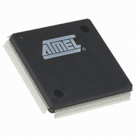
AT91RM9200-QI-002 Atmel, AT91RM9200-QI-002 Datasheet - Page 686

AT91RM9200-QI-002
Manufacturer Part Number
AT91RM9200-QI-002
Description
IC ARM9 MCU 208 PQFP
Manufacturer
Atmel
Series
AT91SAMr
Datasheets
1.AT91RM9200-EK.pdf
(41 pages)
2.AT91RM9200-DK.pdf
(2 pages)
3.AT91RM9200-QU-002.pdf
(701 pages)
Specifications of AT91RM9200-QI-002
Core Processor
ARM9
Core Size
16/32-Bit
Speed
180MHz
Connectivity
EBI/EMI, Ethernet, I²C, MMC, SPI, SSC, UART/USART, USB
Peripherals
POR
Number Of I /o
122
Program Memory Size
128KB (128K x 8)
Program Memory Type
ROM
Ram Size
48K x 8
Voltage - Supply (vcc/vdd)
1.65 V ~ 1.95 V
Oscillator Type
Internal
Operating Temperature
-40°C ~ 85°C
Package / Case
208-MQFP, 208-PQFP
Lead Free Status / RoHS Status
Contains lead / RoHS non-compliant
Eeprom Size
-
Data Converters
-
Available stocks
Company
Part Number
Manufacturer
Quantity
Price
Company:
Part Number:
AT91RM9200-QI-002 SL383
Manufacturer:
Atmel
Quantity:
10 000
- Current page: 686 of 701
- Download datasheet (10Mb)
686
Page
Page 270
Page 271
Page 272
Page 273
Page 276
Page 277
Page 278
Page 279
Page 280
Page 281
Page 282
Page 283
Page 284
Page 312
Page 331
Page 343
Page 358
Page 368
Page 391
Page 452
Page 460
Page 596
Page 598
Page 599
Page 601
Page 614
AT91RM9200
Version B Changes Since Last Issue (Continued)
Changed register names in Table 61: PMC Register Mapping: PMC_MOR to CKGR_MOR, PMC_MCFR to
CKGR_MCFR, PMC_PLLAR to CKGR_PLLAR and PCM_PLLBR to CKGR_PLLBR. Remove registers
PMC_PCK4, PMC_PCK5, PMC_PCK6 and PMC_PCK7 (addresses 0x0050 to 0x005C).
In register PMC_SCER, deleted bits PCK7 to PCK4, fields 15 to 12. All bit names updated to include “Enable”. In
UHP bit description, deleted reference to 12 MHz clock.
In register PMC_SCDR, deleted bits PCK7 to PCK4, fields 15 to 12. All bit names updated to include “Disable”. In
UHP bit description, deleted reference to 12 MHz clock.
In register PMC_SCSR, deleted bits PCK7 to PCK4, fields 15 to 12. All bit names updated to include “Status”. In
UHP bit description, corrected to read “USB Host Port”.
Changed register name to PMC Clock Generator Main Oscillator Register. MOSCEN bit description changed to
include information on Main Clock signal and crystal connection. OSCOUNT bit description changed to remove
multiplication factor for Slow Clock cycles.
Changed register name to PMC Clock Generator Main Clock Frequency Register. Corrected in MAINRDY field
description reference to MAINF.
Changed register name to PMC Clock Generator PLL A Register. In OUTA and MULA bits, changed references to
PLLA Output to PLL A Clock.
Changed register name to PMC Clock Generator PLL B Register. In OUTB and MULB bits, changed references to
PLLB Output to PLL B Clock. Changed bit description for USB_96M.
In PMC_MCKR, new clock source selections specified for CSS. MDIV bit condition added.
In PMC_PCK0 to PMC_PCK3, new clock source selections specified for CSS.
In PMC_IER and PMC_IDR, bits PCK7RDY, PCK6RDY, PCK5RDY and PCK4RDY removed.
In PMC_SR, bits PCK7RDY, PCK6RDY, PCK5RDY and PCK4RDY removed.
In PMC_IMR, bits PCK7RDY, PCK6RDY, PCK5RDY and PCK4RDY removed.
Added Note to Figure 135.
In DBGU Chip ID Register, corrected NVPTYP field to 000 for ROM.
In Table 67: PIO Register Mapping, PIO_OWSR access changed to read-only.
In PIO_OWSR, access changed to read-only.
Changed all references from CPHA to NCPHA. Updated Figures 159 and 160 for clarity.
In CHDIV and CLDIV bit descriptions in register TWI_CWGR, corrected equations for calculation of SCL high and
low periods. In CHDIV, CLDIV and CKDIV bit descriptions in register TWI_CWGR, SCL replaced by TWCK.
Updated Figure 214, Transmit Frame Format in Continuous Mode. Updated Figure 215, Receive Frame Format in
Continuous Mode.
In register SSC_RFMR, new description of bit DATLEN.
In Table 109, DC Characteristics, changed conditions for Static Current.
New consumption figures in Table 113 and Table 114.
In Table 115: 32 kHz Oscillator Characteristics, V
Oscillator Characteristics, V
Characteristics, corrected errors in Pump current max/min values.
In Table 120: Switching Characteristics in Full Speed, min/max values for Rise/Fall Time Matching added.
In Table 125: SDRAMC Signals, changed min values for SDRAMC
DDPLL
defined in Startup Time conditions. In Table 117: Phase Lock Loop
DDOSC
defined in Startup Time conditions. In Table 116: Main
23
to SDRAMC
28
.
1768I–ATARM–09-Jul-09
Related parts for AT91RM9200-QI-002
Image
Part Number
Description
Manufacturer
Datasheet
Request
R

Part Number:
Description:
Manufacturer:
ATMEL Corporation
Datasheet:

Part Number:
Description:
IC ARM MCU 16BIT 128K 256BGA
Manufacturer:
Atmel
Datasheet:

Part Number:
Description:
DEVEL KIT
Manufacturer:
Atmel
Datasheet:

Part Number:
Description:
KIT DEVELOPMENT AT91RM9200
Manufacturer:
Atmel
Datasheet:

Part Number:
Description:
IC ARM9 MCU 208 PQFP
Manufacturer:
Atmel
Datasheet:

Part Number:
Description:
IC ARM9 MCU 256 BGA
Manufacturer:
Atmel
Datasheet:

Part Number:
Description:
IC ARM MCU 16BIT 128K 208PQFP
Manufacturer:
Atmel
Datasheet:

Part Number:
Description:
AT91RM9200 Development Kit
Manufacturer:
ATMEL Corporation
Datasheet:

Part Number:
Description:
DEV KIT FOR AVR/AVR32
Manufacturer:
Atmel
Datasheet:

Part Number:
Description:
INTERVAL AND WIPE/WASH WIPER CONTROL IC WITH DELAY
Manufacturer:
ATMEL Corporation
Datasheet:

Part Number:
Description:
Low-Voltage Voice-Switched IC for Hands-Free Operation
Manufacturer:
ATMEL Corporation
Datasheet:

Part Number:
Description:
MONOLITHIC INTEGRATED FEATUREPHONE CIRCUIT
Manufacturer:
ATMEL Corporation
Datasheet:

Part Number:
Description:
AM-FM Receiver IC U4255BM-M
Manufacturer:
ATMEL Corporation
Datasheet:


