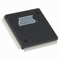
AT91RM9200-QI-002 Atmel, AT91RM9200-QI-002 Datasheet - Page 396

AT91RM9200-QI-002
Manufacturer Part Number
AT91RM9200-QI-002
Description
IC ARM9 MCU 208 PQFP
Manufacturer
Atmel
Series
AT91SAMr
Datasheets
1.AT91RM9200-EK.pdf
(41 pages)
2.AT91RM9200-DK.pdf
(2 pages)
3.AT91RM9200-QU-002.pdf
(701 pages)
Specifications of AT91RM9200-QI-002
Core Processor
ARM9
Core Size
16/32-Bit
Speed
180MHz
Connectivity
EBI/EMI, Ethernet, I²C, MMC, SPI, SSC, UART/USART, USB
Peripherals
POR
Number Of I /o
122
Program Memory Size
128KB (128K x 8)
Program Memory Type
ROM
Ram Size
48K x 8
Voltage - Supply (vcc/vdd)
1.65 V ~ 1.95 V
Oscillator Type
Internal
Operating Temperature
-40°C ~ 85°C
Package / Case
208-MQFP, 208-PQFP
Lead Free Status / RoHS Status
Contains lead / RoHS non-compliant
Eeprom Size
-
Data Converters
-
Available stocks
Company
Part Number
Manufacturer
Quantity
Price
Company:
Part Number:
AT91RM9200-QI-002 SL383
Manufacturer:
Atmel
Quantity:
10 000
- Current page: 396 of 701
- Download datasheet (10Mb)
29.4
29.4.1
29.4.2
29.4.3
29.5
29.5.1
396
Product Dependencies
Functional Description
AT91RM9200
I/O Lines
Power Management
Interrupt
Transfer Format
Table 29-1.
Both TWD and TWCK are bi-directional lines, connected to a positive supply voltage via a cur-
rent source or pull-up resistor (see
are high. The output stages of devices connected to the bus must have an open-drain or open-
collector to perform the wired-AND function.
TWD and TWCK pins may be multiplexed with PIO lines. To enable the TWI, the programmer
must perform the following steps:
The TWI interface may be clocked through the Power Management Controller (PMC), thus the
programmer must first configure the PMC to enable the TWI clock.
The TWI interface has an interrupt line connected to the Advanced Interrupt Controller (AIC). In
order to handle interrupts, the AIC must be programmed before configuring the TWI.
The data put on the TWD line must be eight bits long. Data is transferred MSB first; each byte
must be followed by an acknowledgement. The number of bytes per transfer is unlimited (see
Figure 29-4 on page
Each transfer begins with a START condition and terminates with a STOP condition (see
29-3 on page
Pin Name
TWD
TWCK
• Program the PIO controller to:
• Enable the peripheral clock.
• A high-to-low transition on the TWD line while TWCK is high defines the START condition.
• A low-to-high transition on the TWD line while TWCK is high defines a STOP condition.
– Dedicate TWD and TWCK as peripheral lines.
– Define TWD and TWCK as open-drain.
397).
I/O Lines Description
397).
Pin Description
Two-wire Serial Data
Two-wire Serial Clock
Figure 29-2 on page
395). When the bus is free, both lines
Input/Output
Input/Output
1768I–ATARM–09-Jul-09
Type
Figure
Related parts for AT91RM9200-QI-002
Image
Part Number
Description
Manufacturer
Datasheet
Request
R

Part Number:
Description:
Manufacturer:
ATMEL Corporation
Datasheet:

Part Number:
Description:
IC ARM MCU 16BIT 128K 256BGA
Manufacturer:
Atmel
Datasheet:

Part Number:
Description:
DEVEL KIT
Manufacturer:
Atmel
Datasheet:

Part Number:
Description:
KIT DEVELOPMENT AT91RM9200
Manufacturer:
Atmel
Datasheet:

Part Number:
Description:
IC ARM9 MCU 208 PQFP
Manufacturer:
Atmel
Datasheet:

Part Number:
Description:
IC ARM9 MCU 256 BGA
Manufacturer:
Atmel
Datasheet:

Part Number:
Description:
IC ARM MCU 16BIT 128K 208PQFP
Manufacturer:
Atmel
Datasheet:

Part Number:
Description:
AT91RM9200 Development Kit
Manufacturer:
ATMEL Corporation
Datasheet:

Part Number:
Description:
DEV KIT FOR AVR/AVR32
Manufacturer:
Atmel
Datasheet:

Part Number:
Description:
INTERVAL AND WIPE/WASH WIPER CONTROL IC WITH DELAY
Manufacturer:
ATMEL Corporation
Datasheet:

Part Number:
Description:
Low-Voltage Voice-Switched IC for Hands-Free Operation
Manufacturer:
ATMEL Corporation
Datasheet:

Part Number:
Description:
MONOLITHIC INTEGRATED FEATUREPHONE CIRCUIT
Manufacturer:
ATMEL Corporation
Datasheet:

Part Number:
Description:
AM-FM Receiver IC U4255BM-M
Manufacturer:
ATMEL Corporation
Datasheet:


