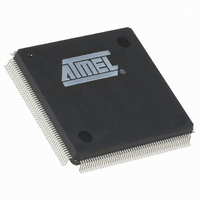
AT91RM9200-QI-002 Atmel, AT91RM9200-QI-002 Datasheet - Page 457

AT91RM9200-QI-002
Manufacturer Part Number
AT91RM9200-QI-002
Description
IC ARM9 MCU 208 PQFP
Manufacturer
Atmel
Series
AT91SAMr
Datasheets
1.AT91RM9200-EK.pdf
(41 pages)
2.AT91RM9200-DK.pdf
(2 pages)
3.AT91RM9200-QU-002.pdf
(701 pages)
Specifications of AT91RM9200-QI-002
Core Processor
ARM9
Core Size
16/32-Bit
Speed
180MHz
Connectivity
EBI/EMI, Ethernet, I²C, MMC, SPI, SSC, UART/USART, USB
Peripherals
POR
Number Of I /o
122
Program Memory Size
128KB (128K x 8)
Program Memory Type
ROM
Ram Size
48K x 8
Voltage - Supply (vcc/vdd)
1.65 V ~ 1.95 V
Oscillator Type
Internal
Operating Temperature
-40°C ~ 85°C
Package / Case
208-MQFP, 208-PQFP
Lead Free Status / RoHS Status
Contains lead / RoHS non-compliant
Eeprom Size
-
Data Converters
-
Available stocks
Company
Part Number
Manufacturer
Quantity
Price
Company:
Part Number:
AT91RM9200-QI-002 SL383
Manufacturer:
Atmel
Quantity:
10 000
- Current page: 457 of 701
- Download datasheet (10Mb)
31.4
31.5
31.5.1
31.5.2
31.5.3
31.6
1768I–ATARM–09-Jul-09
Pin Name List
Product Dependencies
Functional Description
I/O Lines
Power Management
Interrupt
Table 31-1.
The pins used for interfacing the compliant external devices may be multiplexed with PIO lines.
Before using the SSC receiver, the PIO controller must be configured to dedicate the SSC
receiver I/O lines to the SSC peripheral mode.
Before using the SSC transmitter, the PIO controller must be configured to dedicate the SSC
transmitter I/O lines to the SSC peripheral mode.
The SSC is not continuously clocked. The SSC interface may be clocked through the Power
Management Controller (PMC), therefore the programmer must first configure the PMC to
enable the SSC clock.
The SSC interface has an interrupt line connected to the Advanced Interrupt Controller (AIC).
Handling interrupts requires programming the AIC before configuring the SSC.
All SSC interrupts can be enabled/disabled configuring the SSC Interrupt mask register. Each
pending and unmasked SSC interrupt will assert the SSC interrupt line. The SSC interrupt ser-
vice routine can get the interrupt origin by reading the SSC interrupt status register.
This chapter contains the functional description of the following: SSC Functional Block, Clock
Management, Data format, Start, Transmitter, Receiver and Frame Sync.
The receiver and transmitter operate separately. However, they can work synchronously by pro-
gramming the receiver to use the transmit clock and/or to start a data transfer when transmission
starts. Alternatively, this can be done by programming the transmitter to use the receive clock
and/or to start a data transfer when reception starts. The transmitter and the receiver can be pro-
grammed to operate with the clock signals provided on either the TK or RK pins. This allows the
SSC to support many slave-mode data transfers. The maximum clock speed allowed on the TK
and RK pins is the master clock divided by 2. Each level of the clock must be stable for at least
two master clock periods.
Pin Name
RF
RK
RD
TF
TK
TD
I/O Lines Description
Pin Description
Receiver Frame Synchro
Receiver Clock
Receiver Data
Transmitter Frame Synchro
Transmitter Clock
Transmitter Data
AT91RM9200
Input/Output
Input/Output
Input/Output
Input/Output
Output
Type
Input
457
Related parts for AT91RM9200-QI-002
Image
Part Number
Description
Manufacturer
Datasheet
Request
R

Part Number:
Description:
Manufacturer:
ATMEL Corporation
Datasheet:

Part Number:
Description:
IC ARM MCU 16BIT 128K 256BGA
Manufacturer:
Atmel
Datasheet:

Part Number:
Description:
DEVEL KIT
Manufacturer:
Atmel
Datasheet:

Part Number:
Description:
KIT DEVELOPMENT AT91RM9200
Manufacturer:
Atmel
Datasheet:

Part Number:
Description:
IC ARM9 MCU 208 PQFP
Manufacturer:
Atmel
Datasheet:

Part Number:
Description:
IC ARM9 MCU 256 BGA
Manufacturer:
Atmel
Datasheet:

Part Number:
Description:
IC ARM MCU 16BIT 128K 208PQFP
Manufacturer:
Atmel
Datasheet:

Part Number:
Description:
AT91RM9200 Development Kit
Manufacturer:
ATMEL Corporation
Datasheet:

Part Number:
Description:
DEV KIT FOR AVR/AVR32
Manufacturer:
Atmel
Datasheet:

Part Number:
Description:
INTERVAL AND WIPE/WASH WIPER CONTROL IC WITH DELAY
Manufacturer:
ATMEL Corporation
Datasheet:

Part Number:
Description:
Low-Voltage Voice-Switched IC for Hands-Free Operation
Manufacturer:
ATMEL Corporation
Datasheet:

Part Number:
Description:
MONOLITHIC INTEGRATED FEATUREPHONE CIRCUIT
Manufacturer:
ATMEL Corporation
Datasheet:

Part Number:
Description:
AM-FM Receiver IC U4255BM-M
Manufacturer:
ATMEL Corporation
Datasheet:


