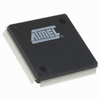
AT91RM9200-QI-002 Atmel, AT91RM9200-QI-002 Datasheet - Page 219

AT91RM9200-QI-002
Manufacturer Part Number
AT91RM9200-QI-002
Description
IC ARM9 MCU 208 PQFP
Manufacturer
Atmel
Series
AT91SAMr
Datasheets
1.AT91RM9200-EK.pdf
(41 pages)
2.AT91RM9200-DK.pdf
(2 pages)
3.AT91RM9200-QU-002.pdf
(701 pages)
Specifications of AT91RM9200-QI-002
Core Processor
ARM9
Core Size
16/32-Bit
Speed
180MHz
Connectivity
EBI/EMI, Ethernet, I²C, MMC, SPI, SSC, UART/USART, USB
Peripherals
POR
Number Of I /o
122
Program Memory Size
128KB (128K x 8)
Program Memory Type
ROM
Ram Size
48K x 8
Voltage - Supply (vcc/vdd)
1.65 V ~ 1.95 V
Oscillator Type
Internal
Operating Temperature
-40°C ~ 85°C
Package / Case
208-MQFP, 208-PQFP
Lead Free Status / RoHS Status
Contains lead / RoHS non-compliant
Eeprom Size
-
Data Converters
-
Available stocks
Company
Part Number
Manufacturer
Quantity
Price
Company:
Part Number:
AT91RM9200-QI-002 SL383
Manufacturer:
Atmel
Quantity:
10 000
- Current page: 219 of 701
- Download datasheet (10Mb)
1768I–ATARM–09-Jul-09
The BFC performs only half-word write requests. Write requests for bytes or words are ignored
by the BFC.
For any access in the address space, the address is driven on the address bus while a pulse is
driven on the BFAVD signal (see
Burst Flash address is also driven on the data bus if the multiplexed data and address bus
options are enabled.
The Address Valid Latency (AVL) determines the length of the pulses as a number of Master
Clock cycles. The AVL field
as the Address Valid Latency minus 1. Waveforms in
on page 221
After a read access to the Burst Flash, it takes Output Enable Latency (OEL) cycles for the Burst
Flash device to release the data bus. The OEL field
on page 227.
trollers from using the Data Bus until it is released by the Burst Flash device.
In
inserted between the read and write accesses. The Burst Flash device must release the data
bus before the BFC can drive the address. As shown in
are not multiplexed, the write access can start as soon as the read access ends. In the same
way, the OEL has no impact when a read follows a write access.
Waveforms in
Burst Flash Controller Clock even though the BFCK pin is driven low in Asynchronous Mode.
The BFCC field
of the burst Flash speed and must also be programmed in Asynchronous Mode.
• For write access, the signal BFWE is asserted in the following BFCK clock cycle.
• For read access, the signal BFOE is asserted one cycle later. This additional cycle in read
• In read access, the access finishes with the rising edge of BFOE.
• In write access, data and address lines are released one half cycle after the rising edge of
Figure 20-4 on page 220
accesses has been inserted to switch the I/O pad direction so as to avoid conflict on the Burst
Flash data bus when address and data busses are multiplexed.
BFWE.
show the AVL field definition in read and write accesses.
gives the OEL expressed in BFCK Clock cycles. This prevents other memory con-
Figure 20-4 on page 220
See “Burst Flash Controller Mode Register” on page
(Figure 20-4 on page
(multiplexed address and data busses), one idle cycle (OEL = 1) is
See “Burst Flash Controller Mode Register” on page 227.
Figure 20-4 on page
below and
220).
Figure 20-5 on page 221
See “Burst Flash Controller Mode Register”
Figure 20-4 on page 220
220, and
Figure 20-5 on page
Figure 20-5 on page
227.is used as a measure
AT91RM9200
221, where busses
are related to the
and
Figure 20-5
221). The
is coded
219
Related parts for AT91RM9200-QI-002
Image
Part Number
Description
Manufacturer
Datasheet
Request
R

Part Number:
Description:
Manufacturer:
ATMEL Corporation
Datasheet:

Part Number:
Description:
IC ARM MCU 16BIT 128K 256BGA
Manufacturer:
Atmel
Datasheet:

Part Number:
Description:
DEVEL KIT
Manufacturer:
Atmel
Datasheet:

Part Number:
Description:
KIT DEVELOPMENT AT91RM9200
Manufacturer:
Atmel
Datasheet:

Part Number:
Description:
IC ARM9 MCU 208 PQFP
Manufacturer:
Atmel
Datasheet:

Part Number:
Description:
IC ARM9 MCU 256 BGA
Manufacturer:
Atmel
Datasheet:

Part Number:
Description:
IC ARM MCU 16BIT 128K 208PQFP
Manufacturer:
Atmel
Datasheet:

Part Number:
Description:
AT91RM9200 Development Kit
Manufacturer:
ATMEL Corporation
Datasheet:

Part Number:
Description:
DEV KIT FOR AVR/AVR32
Manufacturer:
Atmel
Datasheet:

Part Number:
Description:
INTERVAL AND WIPE/WASH WIPER CONTROL IC WITH DELAY
Manufacturer:
ATMEL Corporation
Datasheet:

Part Number:
Description:
Low-Voltage Voice-Switched IC for Hands-Free Operation
Manufacturer:
ATMEL Corporation
Datasheet:

Part Number:
Description:
MONOLITHIC INTEGRATED FEATUREPHONE CIRCUIT
Manufacturer:
ATMEL Corporation
Datasheet:

Part Number:
Description:
AM-FM Receiver IC U4255BM-M
Manufacturer:
ATMEL Corporation
Datasheet:


