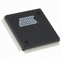
AT91RM9200-QI-002 Atmel, AT91RM9200-QI-002 Datasheet - Page 375

AT91RM9200-QI-002
Manufacturer Part Number
AT91RM9200-QI-002
Description
IC ARM9 MCU 208 PQFP
Manufacturer
Atmel
Series
AT91SAMr
Datasheets
1.AT91RM9200-EK.pdf
(41 pages)
2.AT91RM9200-DK.pdf
(2 pages)
3.AT91RM9200-QU-002.pdf
(701 pages)
Specifications of AT91RM9200-QI-002
Core Processor
ARM9
Core Size
16/32-Bit
Speed
180MHz
Connectivity
EBI/EMI, Ethernet, I²C, MMC, SPI, SSC, UART/USART, USB
Peripherals
POR
Number Of I /o
122
Program Memory Size
128KB (128K x 8)
Program Memory Type
ROM
Ram Size
48K x 8
Voltage - Supply (vcc/vdd)
1.65 V ~ 1.95 V
Oscillator Type
Internal
Operating Temperature
-40°C ~ 85°C
Package / Case
208-MQFP, 208-PQFP
Lead Free Status / RoHS Status
Contains lead / RoHS non-compliant
Eeprom Size
-
Data Converters
-
Available stocks
Company
Part Number
Manufacturer
Quantity
Price
Company:
Part Number:
AT91RM9200-QI-002 SL383
Manufacturer:
Atmel
Quantity:
10 000
- Current page: 375 of 701
- Download datasheet (10Mb)
28.5.1.2
28.5.1.3
28.5.1.4
1768I–ATARM–09-Jul-09
Variable Peripheral Select
Chip Selects
Clock Generation and Transfer Delays
Variable Peripheral Select is activated by setting bit PS to one. The PCS field in SPI_TDR is
used to select the destination peripheral. The data transfer characteristics are changed when
the selected peripheral changes, according to the associated chip select register.
The PCS field in the SPI_MR has no effect.
This option is only available when the SPI is programmed in Master Mode.
The Chip Select lines are driven by the SPI only if it is programmed in Master Mode. These lines
are used to select the destination peripheral. The PCSDEC field in SPI_MR (Mode Register)
selects one to four peripherals (PCSDEC = 0) or up to 15 peripherals (PCSDEC = 1).
If Variable Peripheral Select is active, the chip select signals are defined for each transfer in the
PCS field in SPI_TDR. Chip select signals can thus be defined independently for each transfer.
If Fixed Peripheral Select is active, Chip Select signals are defined for all transfers by the field
PCS in SPI_MR. If a transfer with a new peripheral is necessary, the software must wait until the
current transfer is completed, then change the value of PCS in SPI_MR before writing new data
in SPI_TDR.
The value on the NPCS pins at the end of each transfer can be read in the SPI_RDR (Receive
Data Register).
By default, all NPCS signals are high (equal to one) before and after each transfer.
The SPI Baud rate clock is generated by dividing the Master Clock (MCK) or the Master Clock
divided by 32 (if DIV32 is set in the Mode Register) by a value between 4 and 510. The divisor is
defined in the SCBR field in each Chip Select Register. The transfer speed can thus be defined
independently for each chip select signal.
Figure 28-3
selects. Three delays can be programmed to modify the transfer waveforms:
These delays allow the SPI to be adapted to the interfaced peripherals and their speed and bus
release time.
• Delay between chip selects, programmable only once for all the chip selects by writing the
• Delay before SPCK, independently programmable for each chip select by writing the field
• Delay between consecutive transfers, independently programmable for each chip select by
field DLYBCS in the Mode Register. Allows insertion of a delay between release of one chip
select and before assertion of a new one.
DLYBS. Allows the start of SPCK to be delayed until after the chip select has been asserted.
writing the field DLYBCT. Allows insertion of a delay between two transfers occurring on the
same chip select
shows a chip select transfer change and consecutive transfers on the same chip
AT91RM9200
375
Related parts for AT91RM9200-QI-002
Image
Part Number
Description
Manufacturer
Datasheet
Request
R

Part Number:
Description:
Manufacturer:
ATMEL Corporation
Datasheet:

Part Number:
Description:
IC ARM MCU 16BIT 128K 256BGA
Manufacturer:
Atmel
Datasheet:

Part Number:
Description:
DEVEL KIT
Manufacturer:
Atmel
Datasheet:

Part Number:
Description:
KIT DEVELOPMENT AT91RM9200
Manufacturer:
Atmel
Datasheet:

Part Number:
Description:
IC ARM9 MCU 208 PQFP
Manufacturer:
Atmel
Datasheet:

Part Number:
Description:
IC ARM9 MCU 256 BGA
Manufacturer:
Atmel
Datasheet:

Part Number:
Description:
IC ARM MCU 16BIT 128K 208PQFP
Manufacturer:
Atmel
Datasheet:

Part Number:
Description:
AT91RM9200 Development Kit
Manufacturer:
ATMEL Corporation
Datasheet:

Part Number:
Description:
DEV KIT FOR AVR/AVR32
Manufacturer:
Atmel
Datasheet:

Part Number:
Description:
INTERVAL AND WIPE/WASH WIPER CONTROL IC WITH DELAY
Manufacturer:
ATMEL Corporation
Datasheet:

Part Number:
Description:
Low-Voltage Voice-Switched IC for Hands-Free Operation
Manufacturer:
ATMEL Corporation
Datasheet:

Part Number:
Description:
MONOLITHIC INTEGRATED FEATUREPHONE CIRCUIT
Manufacturer:
ATMEL Corporation
Datasheet:

Part Number:
Description:
AM-FM Receiver IC U4255BM-M
Manufacturer:
ATMEL Corporation
Datasheet:


