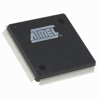
AT91RM9200-QI-002 Atmel, AT91RM9200-QI-002 Datasheet - Page 140

AT91RM9200-QI-002
Manufacturer Part Number
AT91RM9200-QI-002
Description
IC ARM9 MCU 208 PQFP
Manufacturer
Atmel
Series
AT91SAMr
Datasheets
1.AT91RM9200-EK.pdf
(41 pages)
2.AT91RM9200-DK.pdf
(2 pages)
3.AT91RM9200-QU-002.pdf
(701 pages)
Specifications of AT91RM9200-QI-002
Core Processor
ARM9
Core Size
16/32-Bit
Speed
180MHz
Connectivity
EBI/EMI, Ethernet, I²C, MMC, SPI, SSC, UART/USART, USB
Peripherals
POR
Number Of I /o
122
Program Memory Size
128KB (128K x 8)
Program Memory Type
ROM
Ram Size
48K x 8
Voltage - Supply (vcc/vdd)
1.65 V ~ 1.95 V
Oscillator Type
Internal
Operating Temperature
-40°C ~ 85°C
Package / Case
208-MQFP, 208-PQFP
Lead Free Status / RoHS Status
Contains lead / RoHS non-compliant
Eeprom Size
-
Data Converters
-
Available stocks
Company
Part Number
Manufacturer
Quantity
Price
Company:
Part Number:
AT91RM9200-QI-002 SL383
Manufacturer:
Atmel
Quantity:
10 000
- Current page: 140 of 701
- Download datasheet (10Mb)
17.5
17.5.1
17.6
17.6.1
17.6.2
17.6.3
17.6.4
140
Product Dependencies
Functional Description
AT91RM9200
I/O Lines
Bus Multiplexing
Pull-up Control
Static Memory Controller
SDRAM Controller
The pins used for interfacing the External Bus Interface may be multiplexed with the PIO lines.
The programmer must first program the PIO controller to assign the External Bus Interface pins
to their peripheral function. If I/O lines of the External Bus Interface are not used by the applica-
tion, they can be used for other purposes by the PIO Controller.
The EBI transfers data between the internal ASB Bus (handled by the Memory Controller) and
the external memories or peripheral devices. It controls the waveforms and the parameters of
the external address, data and control busses and is composed of the following elements:
The EBI offers a complete set of control signals that share the 32-bit data lines, the address
lines of up to 26 bits and the control signals through a multiplex logic operating in function of the
memory area requests.
Multiplexing is specifically organized in order to guarantee the maintenance of the address and
output control lines at a stable state while no external access is being performed. Multiplexing is
also designed to respect the data float times defined in the Memory Controllers. Furthermore,
refresh cycles of the SDRAM are executed independently by the SDRAM Controller without
delaying the other external Memory Controller accesses. Lastly, it prevents burst accesses on
the same page of a burst Flash from being interrupted which avoids the need to restart a high-
latency first access.
The EBI permits enabling of on-chip pull-up resistors on the data bus lines not multiplexed with
the PIO Controller lines. The pull-up resistors are enabled after reset. Setting the DBPUC bit dis-
ables the pull-up resistors on the D0 to D15 lines. Enabling the pull-up resistor on the D16 - D31
lines can be performed by programming the appropriate PIO controller.
For information on the Static Memory Controller, refer to the SMC
page
For information on the SDRAM Controller, refer to the SDRAMC description on
“Overview” on page
• The Static Memory Controller (SMC)
• The SDRAM Controller (SDRAMC)
• The Burst Flash Controller (BFC)
• A chip select assignment feature that assigns an ASB address space to the external devices.
• A multiplex controller circuit that shares the pins between the different Memory Controllers.
• Programmable CompactFlash support logic
• Programmable NAND Flash /SmartMedia and support logic
155.
193.
Section 18.1 “Description” on
1768I–ATARM–09-Jul-09
Section 19.1
Related parts for AT91RM9200-QI-002
Image
Part Number
Description
Manufacturer
Datasheet
Request
R

Part Number:
Description:
Manufacturer:
ATMEL Corporation
Datasheet:

Part Number:
Description:
IC ARM MCU 16BIT 128K 256BGA
Manufacturer:
Atmel
Datasheet:

Part Number:
Description:
DEVEL KIT
Manufacturer:
Atmel
Datasheet:

Part Number:
Description:
KIT DEVELOPMENT AT91RM9200
Manufacturer:
Atmel
Datasheet:

Part Number:
Description:
IC ARM9 MCU 208 PQFP
Manufacturer:
Atmel
Datasheet:

Part Number:
Description:
IC ARM9 MCU 256 BGA
Manufacturer:
Atmel
Datasheet:

Part Number:
Description:
IC ARM MCU 16BIT 128K 208PQFP
Manufacturer:
Atmel
Datasheet:

Part Number:
Description:
AT91RM9200 Development Kit
Manufacturer:
ATMEL Corporation
Datasheet:

Part Number:
Description:
DEV KIT FOR AVR/AVR32
Manufacturer:
Atmel
Datasheet:

Part Number:
Description:
INTERVAL AND WIPE/WASH WIPER CONTROL IC WITH DELAY
Manufacturer:
ATMEL Corporation
Datasheet:

Part Number:
Description:
Low-Voltage Voice-Switched IC for Hands-Free Operation
Manufacturer:
ATMEL Corporation
Datasheet:

Part Number:
Description:
MONOLITHIC INTEGRATED FEATUREPHONE CIRCUIT
Manufacturer:
ATMEL Corporation
Datasheet:

Part Number:
Description:
AM-FM Receiver IC U4255BM-M
Manufacturer:
ATMEL Corporation
Datasheet:


