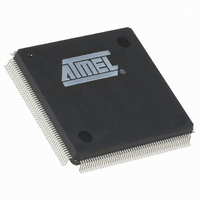
AT91RM9200-QI-002 Atmel, AT91RM9200-QI-002 Datasheet - Page 225

AT91RM9200-QI-002
Manufacturer Part Number
AT91RM9200-QI-002
Description
IC ARM9 MCU 208 PQFP
Manufacturer
Atmel
Series
AT91SAMr
Datasheets
1.AT91RM9200-EK.pdf
(41 pages)
2.AT91RM9200-DK.pdf
(2 pages)
3.AT91RM9200-QU-002.pdf
(701 pages)
Specifications of AT91RM9200-QI-002
Core Processor
ARM9
Core Size
16/32-Bit
Speed
180MHz
Connectivity
EBI/EMI, Ethernet, I²C, MMC, SPI, SSC, UART/USART, USB
Peripherals
POR
Number Of I /o
122
Program Memory Size
128KB (128K x 8)
Program Memory Type
ROM
Ram Size
48K x 8
Voltage - Supply (vcc/vdd)
1.65 V ~ 1.95 V
Oscillator Type
Internal
Operating Temperature
-40°C ~ 85°C
Package / Case
208-MQFP, 208-PQFP
Lead Free Status / RoHS Status
Contains lead / RoHS non-compliant
Eeprom Size
-
Data Converters
-
Available stocks
Company
Part Number
Manufacturer
Quantity
Price
Company:
Part Number:
AT91RM9200-QI-002 SL383
Manufacturer:
Atmel
Quantity:
10 000
- Current page: 225 of 701
- Download datasheet (10Mb)
Figure 20-9. Burst Read in Page Mode
1768I–ATARM–09-Jul-09
Ready Enable Mode
BFAVD
BFBAA
A[24:0]
D[15:0]
D[15:0]
Output
BFWE
BFOE
BFCS
BFCK
Input
(1) A New Page Begins at D8
Burst Read in Page Mode (16 Bytes)
Signal Control Advance Address (BAAEN = 1)
In Page Mode, the BFC stops the current burst and starts a new burst each time the requested
address matches a page boundary.
Data D0 to D10 belong to two separate pages and are accessed through two burst accesses.
This mode is provided for Burst Flash devices that cannot handle continuous burst read (in
which case, a continuous burst access to address D0 would cause the Burst Flash internal
address to wrap around address D0). Page Mode can be disabled by programming a null value
in the PAGES field of the
In Ready Enable Mode (bit RDYEN in the
the BFC uses the Ready Signal (BFRDY) from the burst Flash device as an indicator of the next
data availability. The BFRDY signal must be asserted one BFCK cycle before data is valid. In
Figure 20-10 on page 226
data will not be available on the next rising BFCK edge. The BFRDY signal remains low until ris-
ing at edge (B). D4 is then sampled on edge (C).
AVL
Address (D0)
Sampling
D0
D0
(8 Accesses of 2 Bytes Each)
D1
16-byte Page
…..
…..
“Burst Flash Controller Mode Register” on page
below, the BFRDY signal indicates on edge (A) that the expected D4
D6
Sampling
D7
D7
Figure 20-9 on page 225
D0
“Burst Flash Controller Mode Register” on page
Address Valid Latency = 3 BFCK cycles (AVL field = 2)
Output Enable Latency (OEL) = 1 BFCK cycle
Page Size = 16 Bytes
16-byte Page Boundary
Address (D8)
AVL
illustrates a 16-byte page size.
Sampling
D8
(8 Accesses of 2 Bytes Each)
D8
(1)
AT91RM9200
(1)
D9
227.
16-byte Page
(1)
D10
227),
225
Related parts for AT91RM9200-QI-002
Image
Part Number
Description
Manufacturer
Datasheet
Request
R

Part Number:
Description:
Manufacturer:
ATMEL Corporation
Datasheet:

Part Number:
Description:
IC ARM MCU 16BIT 128K 256BGA
Manufacturer:
Atmel
Datasheet:

Part Number:
Description:
DEVEL KIT
Manufacturer:
Atmel
Datasheet:

Part Number:
Description:
KIT DEVELOPMENT AT91RM9200
Manufacturer:
Atmel
Datasheet:

Part Number:
Description:
IC ARM9 MCU 208 PQFP
Manufacturer:
Atmel
Datasheet:

Part Number:
Description:
IC ARM9 MCU 256 BGA
Manufacturer:
Atmel
Datasheet:

Part Number:
Description:
IC ARM MCU 16BIT 128K 208PQFP
Manufacturer:
Atmel
Datasheet:

Part Number:
Description:
AT91RM9200 Development Kit
Manufacturer:
ATMEL Corporation
Datasheet:

Part Number:
Description:
DEV KIT FOR AVR/AVR32
Manufacturer:
Atmel
Datasheet:

Part Number:
Description:
INTERVAL AND WIPE/WASH WIPER CONTROL IC WITH DELAY
Manufacturer:
ATMEL Corporation
Datasheet:

Part Number:
Description:
Low-Voltage Voice-Switched IC for Hands-Free Operation
Manufacturer:
ATMEL Corporation
Datasheet:

Part Number:
Description:
MONOLITHIC INTEGRATED FEATUREPHONE CIRCUIT
Manufacturer:
ATMEL Corporation
Datasheet:

Part Number:
Description:
AM-FM Receiver IC U4255BM-M
Manufacturer:
ATMEL Corporation
Datasheet:


