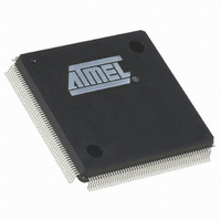
AT91RM9200-QI-002 Atmel, AT91RM9200-QI-002 Datasheet - Page 191

AT91RM9200-QI-002
Manufacturer Part Number
AT91RM9200-QI-002
Description
IC ARM9 MCU 208 PQFP
Manufacturer
Atmel
Series
AT91SAMr
Datasheets
1.AT91RM9200-EK.pdf
(41 pages)
2.AT91RM9200-DK.pdf
(2 pages)
3.AT91RM9200-QU-002.pdf
(701 pages)
Specifications of AT91RM9200-QI-002
Core Processor
ARM9
Core Size
16/32-Bit
Speed
180MHz
Connectivity
EBI/EMI, Ethernet, I²C, MMC, SPI, SSC, UART/USART, USB
Peripherals
POR
Number Of I /o
122
Program Memory Size
128KB (128K x 8)
Program Memory Type
ROM
Ram Size
48K x 8
Voltage - Supply (vcc/vdd)
1.65 V ~ 1.95 V
Oscillator Type
Internal
Operating Temperature
-40°C ~ 85°C
Package / Case
208-MQFP, 208-PQFP
Lead Free Status / RoHS Status
Contains lead / RoHS non-compliant
Eeprom Size
-
Data Converters
-
Available stocks
Company
Part Number
Manufacturer
Quantity
Price
Company:
Part Number:
AT91RM9200-QI-002 SL383
Manufacturer:
Atmel
Quantity:
10 000
- Current page: 191 of 701
- Download datasheet (10Mb)
• DBW: Data Bus Width
• DRP: Data Read Protocol
0: Standard Read Protocol is used.
1: Early Read Protocol is used.
• ACSS: Address to Chip Select Setup
• RWSETUP: Read and Write Signal Setup Time
See definition and description below.
• RWHOLD: Read and Write Signal Hold Time
See definition and description below
Notes:
1768I–ATARM–09-Jul-09
0
0
0
0
1
1
1
1
RWSETUP
1. For a visual description, please refer to
2. In Standard Read Protocol.
3. In Early Read Protocol. (It is not possible to use the parameters RWSETUP or RWHOLD in this mode.)
4. When the ECC Controller is used, RWHOLD must be programmed to 1 at least.
5. If an attempt is made to program the setup parameter as not equal to zero and the hold parameter as equal to zero, with
18-46
WSEN = 0 (0 standard wait state), the SMC does not operate correctly.
0
0
1
1
0
0
1
1
0
0
1
1
0
0
1
1
and
(1) (5)
Figure 18-47 on page
ACSS
DBW
0
1
0
1
0
1
0
1
NRD Setup
½ cycle
0 cycles
1 + ½ cycles
2 + ½ cycles
3 + ½ cycles
4 + ½ cycles
5 + ½ cycles
6 + ½ cycles
7 + ½ cycles
0
1
0
1
0
1
0
1
.
(2)
(3)
or
192.
“Setup and Hold Cycles” on page 168
NWR Setup
½ cycle
1 + ½ cycles
2 + ½ cycles
3 + ½ cycles
4 + ½ cycles
5 + ½ cycles
6 + ½ cycles
7 + ½ cycles
Data Bus Width
Reserved
16-bit
8-bit
Reserved
Chip Select Waveform
Standard, asserted at the beginning of the access and deasserted at the end.
One cycle less at the beginning and the end of the access.
Two cycles less at the beginning and the end of the access.
Three cycles less at the beginning and the end of the access.
0
0
0
0
1
1
1
1
RWHOLD
0
0
1
1
0
0
1
1
(1) (4) (5)
and the diagrams in
0
1
0
1
0
1
0
1
NRD Hold
0
1 cycles
2 cycles
3 cycles
4 cycles
5 cycles
6 cycles
7 cycles
AT91RM9200
Figure 18-45
NWR Hold
½ cycle
1 cycle
2 cycles
3 cycles
4 cycles
5 cycles
6 cycles
7 cycles
and
Figure
191
Related parts for AT91RM9200-QI-002
Image
Part Number
Description
Manufacturer
Datasheet
Request
R

Part Number:
Description:
Manufacturer:
ATMEL Corporation
Datasheet:

Part Number:
Description:
IC ARM MCU 16BIT 128K 256BGA
Manufacturer:
Atmel
Datasheet:

Part Number:
Description:
DEVEL KIT
Manufacturer:
Atmel
Datasheet:

Part Number:
Description:
KIT DEVELOPMENT AT91RM9200
Manufacturer:
Atmel
Datasheet:

Part Number:
Description:
IC ARM9 MCU 208 PQFP
Manufacturer:
Atmel
Datasheet:

Part Number:
Description:
IC ARM9 MCU 256 BGA
Manufacturer:
Atmel
Datasheet:

Part Number:
Description:
IC ARM MCU 16BIT 128K 208PQFP
Manufacturer:
Atmel
Datasheet:

Part Number:
Description:
AT91RM9200 Development Kit
Manufacturer:
ATMEL Corporation
Datasheet:

Part Number:
Description:
DEV KIT FOR AVR/AVR32
Manufacturer:
Atmel
Datasheet:

Part Number:
Description:
INTERVAL AND WIPE/WASH WIPER CONTROL IC WITH DELAY
Manufacturer:
ATMEL Corporation
Datasheet:

Part Number:
Description:
Low-Voltage Voice-Switched IC for Hands-Free Operation
Manufacturer:
ATMEL Corporation
Datasheet:

Part Number:
Description:
MONOLITHIC INTEGRATED FEATUREPHONE CIRCUIT
Manufacturer:
ATMEL Corporation
Datasheet:

Part Number:
Description:
AM-FM Receiver IC U4255BM-M
Manufacturer:
ATMEL Corporation
Datasheet:


