AT91RM9200-QI-002 Atmel, AT91RM9200-QI-002 Datasheet - Page 397

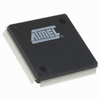
AT91RM9200-QI-002
Manufacturer Part Number
AT91RM9200-QI-002
Description
IC ARM9 MCU 208 PQFP
Manufacturer
Atmel
Series
AT91SAMr
Datasheets
1.AT91RM9200-EK.pdf
(41 pages)
2.AT91RM9200-DK.pdf
(2 pages)
3.AT91RM9200-QU-002.pdf
(701 pages)
Specifications of AT91RM9200-QI-002
Core Processor
ARM9
Core Size
16/32-Bit
Speed
180MHz
Connectivity
EBI/EMI, Ethernet, I²C, MMC, SPI, SSC, UART/USART, USB
Peripherals
POR
Number Of I /o
122
Program Memory Size
128KB (128K x 8)
Program Memory Type
ROM
Ram Size
48K x 8
Voltage - Supply (vcc/vdd)
1.65 V ~ 1.95 V
Oscillator Type
Internal
Operating Temperature
-40°C ~ 85°C
Package / Case
208-MQFP, 208-PQFP
Lead Free Status / RoHS Status
Contains lead / RoHS non-compliant
Eeprom Size
-
Data Converters
-
Available stocks
Company
Part Number
Manufacturer
Quantity
Price
Company:
Part Number:
AT91RM9200-QI-002 SL383
Manufacturer:
Atmel
Quantity:
10 000
- Current page: 397 of 701
- Download datasheet (10Mb)
29.5.2
29.5.3
1768I–ATARM–09-Jul-09
Modes of Operation
Transmitting Data
Figure 29-3.
Figure 29-4. Transfer Format
The TWI has two modes of operations:
The TWI Control Register (TWI_CR) allows configuration of the interface in Master Mode. In this
mode, it generates the clock according to the value programmed in the Clock Waveform Gener-
ator Register (TWI_CWGR). This register defines the TWCK signal completely, enabling the
interface to be adapted to a wide range of clocks.
After the master initiates a Start condition, it sends a 7-bit slave address, configured in the Mas-
ter Mode register (DADR in TWI_MMR), to notify the slave device. The bit following the slave
address indicates the transfer direction (write or read). If this bit is 0, it indicates a write operation
(transmit operation). If the bit is 1, it indicates a request for data read (receive operation).
The TWI transfers require the slave to acknowledge each received byte. During the acknowl-
edge clock pulse, the master releases the data line (HIGH), enabling the slave to pull it down in
order to generate the acknowledge. The master polls the data line during this clock pulse and
sets the NAK bit in the status register if the slave does not acknowledge the byte. As with the
other status bits, an interrupt can be generated if enabled in the interrupt enable register
(TWI_IER). After writing in the transmit-holding register (TWI_THR), setting the START bit in the
control register starts the transmission. The data is shifted in the internal shifter and when an
acknowledge is detected, the TXRDY bit is set until a new write in the TWI_THR (see
6 on page
The read sequence begins by setting the START bit. When the RXRDY bit is set in the status
register, a character has been received in the receive-holding register (TWI_RHR). The RXRDY
bit is reset when reading the TWI_RHR.
The TWI interface performs various transfer formats (7-bit slave address, 10-bit slave address).
The three internal address bytes are configurable through the Master Mode register
(TWI_MMR). If the slave device supports only a 7-bit address, the IADRSZ must be set to 0. For
• Master transmitter mode
• Master receiver mode
398). The master generates a stop condition to end the transfer.
TWD
TWCK
START and STOP Conditions
Start
Address
TWCK
TWD
R/W
Start
Ack
Data
Ack
Data
Stop
AT91RM9200
Ack
Stop
Figure 29-
397
Related parts for AT91RM9200-QI-002
Image
Part Number
Description
Manufacturer
Datasheet
Request
R

Part Number:
Description:
Manufacturer:
ATMEL Corporation
Datasheet:

Part Number:
Description:
IC ARM MCU 16BIT 128K 256BGA
Manufacturer:
Atmel
Datasheet:

Part Number:
Description:
DEVEL KIT
Manufacturer:
Atmel
Datasheet:

Part Number:
Description:
KIT DEVELOPMENT AT91RM9200
Manufacturer:
Atmel
Datasheet:

Part Number:
Description:
IC ARM9 MCU 208 PQFP
Manufacturer:
Atmel
Datasheet:

Part Number:
Description:
IC ARM9 MCU 256 BGA
Manufacturer:
Atmel
Datasheet:

Part Number:
Description:
IC ARM MCU 16BIT 128K 208PQFP
Manufacturer:
Atmel
Datasheet:

Part Number:
Description:
AT91RM9200 Development Kit
Manufacturer:
ATMEL Corporation
Datasheet:

Part Number:
Description:
DEV KIT FOR AVR/AVR32
Manufacturer:
Atmel
Datasheet:

Part Number:
Description:
INTERVAL AND WIPE/WASH WIPER CONTROL IC WITH DELAY
Manufacturer:
ATMEL Corporation
Datasheet:

Part Number:
Description:
Low-Voltage Voice-Switched IC for Hands-Free Operation
Manufacturer:
ATMEL Corporation
Datasheet:

Part Number:
Description:
MONOLITHIC INTEGRATED FEATUREPHONE CIRCUIT
Manufacturer:
ATMEL Corporation
Datasheet:

Part Number:
Description:
AM-FM Receiver IC U4255BM-M
Manufacturer:
ATMEL Corporation
Datasheet:


