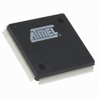
AT91RM9200-QI-002 Atmel, AT91RM9200-QI-002 Datasheet - Page 473

AT91RM9200-QI-002
Manufacturer Part Number
AT91RM9200-QI-002
Description
IC ARM9 MCU 208 PQFP
Manufacturer
Atmel
Series
AT91SAMr
Datasheets
1.AT91RM9200-EK.pdf
(41 pages)
2.AT91RM9200-DK.pdf
(2 pages)
3.AT91RM9200-QU-002.pdf
(701 pages)
Specifications of AT91RM9200-QI-002
Core Processor
ARM9
Core Size
16/32-Bit
Speed
180MHz
Connectivity
EBI/EMI, Ethernet, I²C, MMC, SPI, SSC, UART/USART, USB
Peripherals
POR
Number Of I /o
122
Program Memory Size
128KB (128K x 8)
Program Memory Type
ROM
Ram Size
48K x 8
Voltage - Supply (vcc/vdd)
1.65 V ~ 1.95 V
Oscillator Type
Internal
Operating Temperature
-40°C ~ 85°C
Package / Case
208-MQFP, 208-PQFP
Lead Free Status / RoHS Status
Contains lead / RoHS non-compliant
Eeprom Size
-
Data Converters
-
Available stocks
Company
Part Number
Manufacturer
Quantity
Price
Company:
Part Number:
AT91RM9200-QI-002 SL383
Manufacturer:
Atmel
Quantity:
10 000
- Current page: 473 of 701
- Download datasheet (10Mb)
31.8.4
Register Name:
Access Type:
• DATLEN: Data Length
0x0 is not supported. The value of DATLEN can be set between 0x1 and 0x1F.
The bit stream contains DATLEN + 1 data bits. Moreover, it defines the transfer size performed by the PDC assigned to the
Receiver.
If DATLEN is less than or equal to 7, data transfers are in bytes. If DATLEN is between 8 and 15 (included), half-words are
transferred. For any other value, 32-bit words are transferred.
• LOOP: Loop Mode
0: Normal operating mode.
1: RD is driven by TD, RF is driven by TF and TK drives RK.
• MSBF: Most Significant Bit First
0: The lowest significant bit of the data register is sampled first in the bit stream.
1: The most significant bit of the data register is sampled first in the bit stream.
• DATNB: Data Number per Frame
This field defines the number of data words to be received after each transfer start. If 0, only 1 data word is transferred. Up
to 16 data words can be transferred.
• FSLEN: Receive Frame Sync Length
This field defines the length of the Receive Frame Sync Signal and the number of bits sampled and stored in the Receive
Sync Data Register. Only when FSOS is set on negative or positive pulse.
• FSOS: Receive Frame Sync Output Selection
1768I–ATARM–09-Jul-09
MSBF
0x6-0x7
31
23
15
FSOS
–
–
–
7
0x0
0x1
0x2
0x3
0x4
0x5
SSC Receive Frame Mode Register
Selected Receive Frame Sync Signal
None
Negative Pulse
Positive Pulse
Driven Low during data transfer
Driven High during data transfer
Toggling at each start of data transfer
Reserved
30
22
14
SSC_RFMR
Read/Write
–
–
6
–
FSOS
LOOP
29
21
13
–
–
5
28
20
12
–
–
4
27
19
11
–
3
DATLEN
26
18
10
–
2
FSLEN
DATNB
AT91RM9200
25
17
–
9
1
Undefined
Input-only
RF pin
Output
Output
Output
Output
Output
FSEDGE
24
16
8
0
473
Related parts for AT91RM9200-QI-002
Image
Part Number
Description
Manufacturer
Datasheet
Request
R

Part Number:
Description:
Manufacturer:
ATMEL Corporation
Datasheet:

Part Number:
Description:
IC ARM MCU 16BIT 128K 256BGA
Manufacturer:
Atmel
Datasheet:

Part Number:
Description:
DEVEL KIT
Manufacturer:
Atmel
Datasheet:

Part Number:
Description:
KIT DEVELOPMENT AT91RM9200
Manufacturer:
Atmel
Datasheet:

Part Number:
Description:
IC ARM9 MCU 208 PQFP
Manufacturer:
Atmel
Datasheet:

Part Number:
Description:
IC ARM9 MCU 256 BGA
Manufacturer:
Atmel
Datasheet:

Part Number:
Description:
IC ARM MCU 16BIT 128K 208PQFP
Manufacturer:
Atmel
Datasheet:

Part Number:
Description:
AT91RM9200 Development Kit
Manufacturer:
ATMEL Corporation
Datasheet:

Part Number:
Description:
DEV KIT FOR AVR/AVR32
Manufacturer:
Atmel
Datasheet:

Part Number:
Description:
INTERVAL AND WIPE/WASH WIPER CONTROL IC WITH DELAY
Manufacturer:
ATMEL Corporation
Datasheet:

Part Number:
Description:
Low-Voltage Voice-Switched IC for Hands-Free Operation
Manufacturer:
ATMEL Corporation
Datasheet:

Part Number:
Description:
MONOLITHIC INTEGRATED FEATUREPHONE CIRCUIT
Manufacturer:
ATMEL Corporation
Datasheet:

Part Number:
Description:
AM-FM Receiver IC U4255BM-M
Manufacturer:
ATMEL Corporation
Datasheet:


