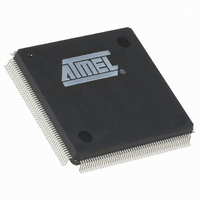
AT91RM9200-QI-002 Atmel, AT91RM9200-QI-002 Datasheet - Page 55

AT91RM9200-QI-002
Manufacturer Part Number
AT91RM9200-QI-002
Description
IC ARM9 MCU 208 PQFP
Manufacturer
Atmel
Series
AT91SAMr
Datasheets
1.AT91RM9200-EK.pdf
(41 pages)
2.AT91RM9200-DK.pdf
(2 pages)
3.AT91RM9200-QU-002.pdf
(701 pages)
Specifications of AT91RM9200-QI-002
Core Processor
ARM9
Core Size
16/32-Bit
Speed
180MHz
Connectivity
EBI/EMI, Ethernet, I²C, MMC, SPI, SSC, UART/USART, USB
Peripherals
POR
Number Of I /o
122
Program Memory Size
128KB (128K x 8)
Program Memory Type
ROM
Ram Size
48K x 8
Voltage - Supply (vcc/vdd)
1.65 V ~ 1.95 V
Oscillator Type
Internal
Operating Temperature
-40°C ~ 85°C
Package / Case
208-MQFP, 208-PQFP
Lead Free Status / RoHS Status
Contains lead / RoHS non-compliant
Eeprom Size
-
Data Converters
-
Available stocks
Company
Part Number
Manufacturer
Quantity
Price
Company:
Part Number:
AT91RM9200-QI-002 SL383
Manufacturer:
Atmel
Quantity:
10 000
- Current page: 55 of 701
- Download datasheet (10Mb)
11.7.9
Access: Write-only
The CP15 Register 8, or Translation Lookaside Buffer (TLB) Operations Register, is used to manage instruction TLBs and
data TLBs.
The TLB operation is selected by opcode_2 and CRm fields in the MCR instruction used to write CP15 Register 8.
Table 11-7.
Below are details of the CP15 Register 8 for TLB operation on MVA format and one single entry.
• mva[31:10]: Modified Virtual Address
The non-defined bits should be zero when written and are unpredictable when read.
Writing other opcode_2 values or CRm values is unpredictable.
Reading from CP15 Register 8 is unpredictable.
1768I–ATARM–09-Jul-09
Function
Invalidate I TLB
Invalidate I TLB single entry (using MVA)
Invalidate D TLB
Invalidate D TLB single entry (using MVA)
Invalidate both Instruction and Data TLB
31
23
15
7
-
CP15 Register 8, TLB Operations Register
TLB Operations
30
22
14
6
-
29
21
13
5
-
mva
28
20
12
4
-
mva
mva
27
19
11
MVA format
MVA format
3
-
Data
SBZ
SBZ
SBZ
26
18
10
2
-
CRm
5
5
6
6
7
AT91RM9200
25
17
9
1
-
-
opcode_2
0
1
0
1
24
16
8
0
-
-
55
Related parts for AT91RM9200-QI-002
Image
Part Number
Description
Manufacturer
Datasheet
Request
R

Part Number:
Description:
Manufacturer:
ATMEL Corporation
Datasheet:

Part Number:
Description:
IC ARM MCU 16BIT 128K 256BGA
Manufacturer:
Atmel
Datasheet:

Part Number:
Description:
DEVEL KIT
Manufacturer:
Atmel
Datasheet:

Part Number:
Description:
KIT DEVELOPMENT AT91RM9200
Manufacturer:
Atmel
Datasheet:

Part Number:
Description:
IC ARM9 MCU 208 PQFP
Manufacturer:
Atmel
Datasheet:

Part Number:
Description:
IC ARM9 MCU 256 BGA
Manufacturer:
Atmel
Datasheet:

Part Number:
Description:
IC ARM MCU 16BIT 128K 208PQFP
Manufacturer:
Atmel
Datasheet:

Part Number:
Description:
AT91RM9200 Development Kit
Manufacturer:
ATMEL Corporation
Datasheet:

Part Number:
Description:
DEV KIT FOR AVR/AVR32
Manufacturer:
Atmel
Datasheet:

Part Number:
Description:
INTERVAL AND WIPE/WASH WIPER CONTROL IC WITH DELAY
Manufacturer:
ATMEL Corporation
Datasheet:

Part Number:
Description:
Low-Voltage Voice-Switched IC for Hands-Free Operation
Manufacturer:
ATMEL Corporation
Datasheet:

Part Number:
Description:
MONOLITHIC INTEGRATED FEATUREPHONE CIRCUIT
Manufacturer:
ATMEL Corporation
Datasheet:

Part Number:
Description:
AM-FM Receiver IC U4255BM-M
Manufacturer:
ATMEL Corporation
Datasheet:


