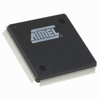
AT91RM9200-QI-002 Atmel, AT91RM9200-QI-002 Datasheet - Page 608

AT91RM9200-QI-002
Manufacturer Part Number
AT91RM9200-QI-002
Description
IC ARM9 MCU 208 PQFP
Manufacturer
Atmel
Series
AT91SAMr
Datasheets
1.AT91RM9200-EK.pdf
(41 pages)
2.AT91RM9200-DK.pdf
(2 pages)
3.AT91RM9200-QU-002.pdf
(701 pages)
Specifications of AT91RM9200-QI-002
Core Processor
ARM9
Core Size
16/32-Bit
Speed
180MHz
Connectivity
EBI/EMI, Ethernet, I²C, MMC, SPI, SSC, UART/USART, USB
Peripherals
POR
Number Of I /o
122
Program Memory Size
128KB (128K x 8)
Program Memory Type
ROM
Ram Size
48K x 8
Voltage - Supply (vcc/vdd)
1.65 V ~ 1.95 V
Oscillator Type
Internal
Operating Temperature
-40°C ~ 85°C
Package / Case
208-MQFP, 208-PQFP
Lead Free Status / RoHS Status
Contains lead / RoHS non-compliant
Eeprom Size
-
Data Converters
-
Available stocks
Company
Part Number
Manufacturer
Quantity
Price
Company:
Part Number:
AT91RM9200-QI-002 SL383
Manufacturer:
Atmel
Quantity:
10 000
- Current page: 608 of 701
- Download datasheet (10Mb)
36.5.4.1
36.5.4.2
608
AT91RM9200
Transmitter Mode
Receiver Mode
The DMA controller performs four types of operations on the ASB bus. In order of priority, these
operations are receive buffer manager read, receive buffer manager write, transmit data DMA
read and receive data DMA write.
Transmit frame data needs to be stored in contiguous memory locations. It does not need to be
word-aligned.
The transmit address register is written with the address of the first byte to be transmitted.
Transmit is initiated by writing the number of bytes to transfer (length) to the transmit control
register.
The transmit channel then reads data from memory 32 bits at a time and places them in the
transmit FIFO.
The transmit block starts frame transmission when three words have been loaded into the FIFO.
The transmit address register must be written before the transmit control register. While a frame
is being transmitted, it is possible to set up one other frame for transmission by writing new val-
ues to the transmit address and control registers. Reading the transmit address register returns
the address of the buffer currently being accessed by the transmit FIFO.
Reading the transmit control register returns the total number of bytes to be transmitted. The
BNQ bit in the Transmit Status Register indicates whether another buffer can be safely queued.
An interrupt is generated whenever this bit is set.
Frame assembly starts by adding preamble and the start frame delimiter. Data is taken from the
transmit FIFO word-by-word. If necessary, padding is added to make the frame length 60 bytes.
The CRC is calculated as a 32-bit polynomial. This is inverted and appended to the end of the
frame, making the frame length a minimum of 64 bytes. The CRC is not appended if the NCRC
bit is set in the transmit control register.
In full-duplex mode, frames are transmitted immediately. Back-to-back frames are transmitted at
least 96 bit times apart to guarantee the inter-frame gap.
In half-duplex mode, the transmitter checks carrier sense. If asserted, it waits for it to de-assert
and then starts transmission after the inter-frame gap of 96 bit-times.
If the collision signal is asserted during transmission, the transmitter transmits a jam sequence
of 32 bits taken from the data register and then retries transmission after the backoff time has
elapsed. An error is indicated and any further attempts aborted if 16 attempts cause collisions.
If transmit DMA underruns, bad CRC is automatically appended using the same mechanism as
jam insertion. Underrun also causes TXER to be asserted.
When a packet is received, it is checked for valid preamble, CRC, alignment, length and
address. If all these criteria are met, the packet is stored successfully in a receive buffer. If at the
end of reception the CRC is bad, then the received buffer is recovered. Each received frame
including CRC is written to a single receive buffer.
Receive buffers are word-aligned and are capable of containing 1518 or 1522 bytes (BIG = 1 in
ETH_CFG) of data (the maximum length of an Ethernet frame).
The start location for each received frame is stored in memory in a list of receive buffer descrip-
tors at a location pointed to by the receive buffer queue pointer register. Each entry in the list
1768I–ATARM–09-Jul-09
Related parts for AT91RM9200-QI-002
Image
Part Number
Description
Manufacturer
Datasheet
Request
R

Part Number:
Description:
Manufacturer:
ATMEL Corporation
Datasheet:

Part Number:
Description:
IC ARM MCU 16BIT 128K 256BGA
Manufacturer:
Atmel
Datasheet:

Part Number:
Description:
DEVEL KIT
Manufacturer:
Atmel
Datasheet:

Part Number:
Description:
KIT DEVELOPMENT AT91RM9200
Manufacturer:
Atmel
Datasheet:

Part Number:
Description:
IC ARM9 MCU 208 PQFP
Manufacturer:
Atmel
Datasheet:

Part Number:
Description:
IC ARM9 MCU 256 BGA
Manufacturer:
Atmel
Datasheet:

Part Number:
Description:
IC ARM MCU 16BIT 128K 208PQFP
Manufacturer:
Atmel
Datasheet:

Part Number:
Description:
AT91RM9200 Development Kit
Manufacturer:
ATMEL Corporation
Datasheet:

Part Number:
Description:
DEV KIT FOR AVR/AVR32
Manufacturer:
Atmel
Datasheet:

Part Number:
Description:
INTERVAL AND WIPE/WASH WIPER CONTROL IC WITH DELAY
Manufacturer:
ATMEL Corporation
Datasheet:

Part Number:
Description:
Low-Voltage Voice-Switched IC for Hands-Free Operation
Manufacturer:
ATMEL Corporation
Datasheet:

Part Number:
Description:
MONOLITHIC INTEGRATED FEATUREPHONE CIRCUIT
Manufacturer:
ATMEL Corporation
Datasheet:

Part Number:
Description:
AM-FM Receiver IC U4255BM-M
Manufacturer:
ATMEL Corporation
Datasheet:


