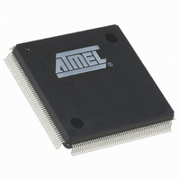
AT91RM9200-QI-002 Atmel, AT91RM9200-QI-002 Datasheet - Page 125

AT91RM9200-QI-002
Manufacturer Part Number
AT91RM9200-QI-002
Description
IC ARM9 MCU 208 PQFP
Manufacturer
Atmel
Series
AT91SAMr
Datasheets
1.AT91RM9200-EK.pdf
(41 pages)
2.AT91RM9200-DK.pdf
(2 pages)
3.AT91RM9200-QU-002.pdf
(701 pages)
Specifications of AT91RM9200-QI-002
Core Processor
ARM9
Core Size
16/32-Bit
Speed
180MHz
Connectivity
EBI/EMI, Ethernet, I²C, MMC, SPI, SSC, UART/USART, USB
Peripherals
POR
Number Of I /o
122
Program Memory Size
128KB (128K x 8)
Program Memory Type
ROM
Ram Size
48K x 8
Voltage - Supply (vcc/vdd)
1.65 V ~ 1.95 V
Oscillator Type
Internal
Operating Temperature
-40°C ~ 85°C
Package / Case
208-MQFP, 208-PQFP
Lead Free Status / RoHS Status
Contains lead / RoHS non-compliant
Eeprom Size
-
Data Converters
-
Available stocks
Company
Part Number
Manufacturer
Quantity
Price
Company:
Part Number:
AT91RM9200-QI-002 SL383
Manufacturer:
Atmel
Quantity:
10 000
- Current page: 125 of 701
- Download datasheet (10Mb)
16.3.2.3
16.3.2.4
16.3.3
1768I–ATARM–09-Jul-09
Remap Command
Internal Memory Area 0
Boot Mode Select
Figure 16-3. Internal Memory Mapping After Remap
Depending on the BMS pin state at reset and as a function of the remap command, the memory
mapped at address 0x0 is different. Before execution of the remap command the on-chip ROM
(BMS = 1) or the 16-bit non-volatile memory connected to external chip select zero (BMS = 0) is
mapped into Internal Memory Area 0. After the remap command, the internal SRAM at address
0x0020 0000 is mapped into Internal Memory Area 0. The memory mapped into Internal Mem-
ory Area 0 is accessible in both its original location and at address 0x0.
The first 32 bytes of Internal Memory Area 0 contain the ARM processor exception vectors.
Table 16-1.
The BMS pin state allows the device to boot out of an internal ROM or out of an external 16-bit
memory connected on the signal NCS0. The input level on the BMS pin during the last 2 clock
cycles before the reset selects the type of boot memory according to the following conditions:
The BMS pin is multiplexed with an I/O line. After reset, this pin can be used as any standard
PIO line.
After execution, the Remap Command causes the Internal SRAM to be accessed through the
Internal Memory Area 0.
As the ARM vectors (Reset, Abort, Data Abort, Prefetch Abort, Undefined Instruction, Interrupt,
and Fast Interrupt) are mapped from address 0x0 to address 0x20, the Remap Command allows
the user to redefine dynamically these vectors under software control.
BMS State
Internal Memory Area 0
• If high, the Internal ROM, which is generally mapped within the Internal Memory Area 1, is
• If low, the External Memory Area 0, which is generally accessible from address 0x10000000,
also accessible through the Internal Memory Area 0
is also accessible through the Internal Memory Area 0.
256M bytes
Internal Memory Area Depending on BMS and the Remap Command
0x0000 0000
0x0010 0000
0x0020 0000
0x0030 0000
0x0FFF FFFF
0x000F FFFF
0x001F FFFF
0x002F FFFF
0x003F FFFF
0x0040 0000
Internal ROM
1
Internal Memory Area 0
Internal Memory Area 1
Internal Memory Area 2
Internal Memory Area 3
Undefined Area
Internal SRAM
USB Host Port
Internal ROM
Before Remap
(Abort)
External Memory Area 0
0
AT91RM9200
252M bytes
1M Byte
1M Byte
1M Byte
1M Byte
After Remap
Internal SRAM
X
125
Related parts for AT91RM9200-QI-002
Image
Part Number
Description
Manufacturer
Datasheet
Request
R

Part Number:
Description:
Manufacturer:
ATMEL Corporation
Datasheet:

Part Number:
Description:
IC ARM MCU 16BIT 128K 256BGA
Manufacturer:
Atmel
Datasheet:

Part Number:
Description:
DEVEL KIT
Manufacturer:
Atmel
Datasheet:

Part Number:
Description:
KIT DEVELOPMENT AT91RM9200
Manufacturer:
Atmel
Datasheet:

Part Number:
Description:
IC ARM9 MCU 208 PQFP
Manufacturer:
Atmel
Datasheet:

Part Number:
Description:
IC ARM9 MCU 256 BGA
Manufacturer:
Atmel
Datasheet:

Part Number:
Description:
IC ARM MCU 16BIT 128K 208PQFP
Manufacturer:
Atmel
Datasheet:

Part Number:
Description:
AT91RM9200 Development Kit
Manufacturer:
ATMEL Corporation
Datasheet:

Part Number:
Description:
DEV KIT FOR AVR/AVR32
Manufacturer:
Atmel
Datasheet:

Part Number:
Description:
INTERVAL AND WIPE/WASH WIPER CONTROL IC WITH DELAY
Manufacturer:
ATMEL Corporation
Datasheet:

Part Number:
Description:
Low-Voltage Voice-Switched IC for Hands-Free Operation
Manufacturer:
ATMEL Corporation
Datasheet:

Part Number:
Description:
MONOLITHIC INTEGRATED FEATUREPHONE CIRCUIT
Manufacturer:
ATMEL Corporation
Datasheet:

Part Number:
Description:
AM-FM Receiver IC U4255BM-M
Manufacturer:
ATMEL Corporation
Datasheet:


