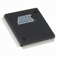
AT91RM9200-QI-002 Atmel, AT91RM9200-QI-002 Datasheet - Page 44

AT91RM9200-QI-002
Manufacturer Part Number
AT91RM9200-QI-002
Description
IC ARM9 MCU 208 PQFP
Manufacturer
Atmel
Series
AT91SAMr
Datasheets
1.AT91RM9200-EK.pdf
(41 pages)
2.AT91RM9200-DK.pdf
(2 pages)
3.AT91RM9200-QU-002.pdf
(701 pages)
Specifications of AT91RM9200-QI-002
Core Processor
ARM9
Core Size
16/32-Bit
Speed
180MHz
Connectivity
EBI/EMI, Ethernet, I²C, MMC, SPI, SSC, UART/USART, USB
Peripherals
POR
Number Of I /o
122
Program Memory Size
128KB (128K x 8)
Program Memory Type
ROM
Ram Size
48K x 8
Voltage - Supply (vcc/vdd)
1.65 V ~ 1.95 V
Oscillator Type
Internal
Operating Temperature
-40°C ~ 85°C
Package / Case
208-MQFP, 208-PQFP
Lead Free Status / RoHS Status
Contains lead / RoHS non-compliant
Eeprom Size
-
Data Converters
-
Available stocks
Company
Part Number
Manufacturer
Quantity
Price
Company:
Part Number:
AT91RM9200-QI-002 SL383
Manufacturer:
Atmel
Quantity:
10 000
- Current page: 44 of 701
- Download datasheet (10Mb)
11.6
11.6.1
11.6.2
11.6.2.1
Write-though Operation
44
Caches, Write Buffers and Physical Address
AT91RM9200
Instruction Cache (ICache)
Data Cache (DCache) and Write Buffer
DCache
The ARM920T includes an Instruction Cache (ICache), a Data Cache (DCache), a write buffer
and a Physical Address (PA) TAG RAM to reduce the effect on main memory bandwidth and
latency performance.
The ARM920T implements separate 16-Kbyte Instruction and 16-Kbyte Data Caches.
The caches and the write buffer are controlled by the CP15 Register 1 (Control), CP15 Register
7 (Cache Operations) and CP15 Register 9 (Cache Lockdown).
The ARM920T includes a 16-Kbyte Instruction Cache (ICache). The ICache has 512 lines of 32
bytes, arranged as a 64-way set associative cache.
Instruction access is subject to MMU permission and translation checks.
If the ICache is enabled with the MMU disabled, all instructions fetched as threats are cachable.
No protection checks are made and the physical address is flat-mapped to the modified virtual
address.
When the ICache is disabled, the cache contents are ignored and all instruction fetches appear
on the AMBA bus.
On reset, the ICache entries are invalidated and the ICache is disabled. For best performance,
ICache should be enabled as soon as possible after reset.
The ICache is enabled by writing 1 to I bit of the CP15 Register 1 and disabled by writing 0 to
this bit. For more details, see
The ICache is organized as eight segments, each containing 64 lines with each line made up of
8 words.The position of the line within the segment is called the index and is numbered from 0 to
63.
A line in the cache is identified by the index and segment. The index is independent of the MVA
(Modified Virtual Address), and the segment is the bit[7:5] of the MVA.
The ARM920T includes a 16-Kbyte data cache (DCache). The DCache has 512 lines of 32
bytes, arranged as a 64-way set associative cache, and uses MVAs translated by CP15 Regis-
ter 13 from the ARM9DTMI core.
The DCache is organized as eight segments, each containing 64 lines with each line made up of
eight words.The position of the line within the segment is called the index and is a number from
0 to 63.
The Write Buffer can hold up to 16 words of data and four separate addresses.
DCache and Write Buffer operations are closely connected as their configuration is set in each
section by the page descriptor in the MMU translation table.
All data accesses are subject to MMU permission and translation checks. Data accesses
aborted by the MMU cannot cause linefill or data access via the AMBA ASB interface.
When a cache hit occurs for a data access, the cache line that contains the data is updated to
contains its value. The new data is also immediately written to the main memory.
“CP15 Register 1, Control” on page
48.
1768I–ATARM–09-Jul-09
Related parts for AT91RM9200-QI-002
Image
Part Number
Description
Manufacturer
Datasheet
Request
R

Part Number:
Description:
Manufacturer:
ATMEL Corporation
Datasheet:

Part Number:
Description:
IC ARM MCU 16BIT 128K 256BGA
Manufacturer:
Atmel
Datasheet:

Part Number:
Description:
DEVEL KIT
Manufacturer:
Atmel
Datasheet:

Part Number:
Description:
KIT DEVELOPMENT AT91RM9200
Manufacturer:
Atmel
Datasheet:

Part Number:
Description:
IC ARM9 MCU 208 PQFP
Manufacturer:
Atmel
Datasheet:

Part Number:
Description:
IC ARM9 MCU 256 BGA
Manufacturer:
Atmel
Datasheet:

Part Number:
Description:
IC ARM MCU 16BIT 128K 208PQFP
Manufacturer:
Atmel
Datasheet:

Part Number:
Description:
AT91RM9200 Development Kit
Manufacturer:
ATMEL Corporation
Datasheet:

Part Number:
Description:
DEV KIT FOR AVR/AVR32
Manufacturer:
Atmel
Datasheet:

Part Number:
Description:
INTERVAL AND WIPE/WASH WIPER CONTROL IC WITH DELAY
Manufacturer:
ATMEL Corporation
Datasheet:

Part Number:
Description:
Low-Voltage Voice-Switched IC for Hands-Free Operation
Manufacturer:
ATMEL Corporation
Datasheet:

Part Number:
Description:
MONOLITHIC INTEGRATED FEATUREPHONE CIRCUIT
Manufacturer:
ATMEL Corporation
Datasheet:

Part Number:
Description:
AM-FM Receiver IC U4255BM-M
Manufacturer:
ATMEL Corporation
Datasheet:


