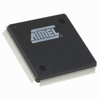
AT91RM9200-QI-002 Atmel, AT91RM9200-QI-002 Datasheet - Page 423

AT91RM9200-QI-002
Manufacturer Part Number
AT91RM9200-QI-002
Description
IC ARM9 MCU 208 PQFP
Manufacturer
Atmel
Series
AT91SAMr
Datasheets
1.AT91RM9200-EK.pdf
(41 pages)
2.AT91RM9200-DK.pdf
(2 pages)
3.AT91RM9200-QU-002.pdf
(701 pages)
Specifications of AT91RM9200-QI-002
Core Processor
ARM9
Core Size
16/32-Bit
Speed
180MHz
Connectivity
EBI/EMI, Ethernet, I²C, MMC, SPI, SSC, UART/USART, USB
Peripherals
POR
Number Of I /o
122
Program Memory Size
128KB (128K x 8)
Program Memory Type
ROM
Ram Size
48K x 8
Voltage - Supply (vcc/vdd)
1.65 V ~ 1.95 V
Oscillator Type
Internal
Operating Temperature
-40°C ~ 85°C
Package / Case
208-MQFP, 208-PQFP
Lead Free Status / RoHS Status
Contains lead / RoHS non-compliant
Eeprom Size
-
Data Converters
-
Available stocks
Company
Part Number
Manufacturer
Quantity
Price
Company:
Part Number:
AT91RM9200-QI-002 SL383
Manufacturer:
Atmel
Quantity:
10 000
- Current page: 423 of 701
- Download datasheet (10Mb)
30.6.3.6
1768I–ATARM–09-Jul-09
Multi-drop Mode
used, the parity generator of the transmitter drives the parity bit at 0 for all characters. The
receiver parity checker reports an error if the parity bit is sampled at 1. If parity is disabled, the
transmitter does not generate any parity bit and the receiver does not report any parity error.
Table 30-6
depending on the configuration of the USART. Because there are two bits at 1, 1 bit is added
when a parity is odd, or 0 is added when a parity is even. I
Table 30-6.
When the receiver detects a parity error, it sets the PARE (Parity Error) bit in the Channel Status
Register (US_CSR). The PARE bit can be cleared by writing the Control Register (US_CR) with
the RSTSTA bit at 1.
Figure 30-11. Parity Error
If the PAR field in the Mode Register (US_MR) is programmed to the value 0x6 or 0x7, the
USART runs in Multi-drop mode. This mode differentiates the data characters and the address
characters. Data is transmitted with the parity bit at 0 and addresses are transmitted with the
parity bit at 1.
If the USART is configured in multi-drop mode, the receiver sets the PARE parity error bit when
the parity bit is high and the transmitter is able to send a character with the parity bit high when
the Control Register is written with the SENDA bit at 1.
To handle parity error, the PARE bit is cleared when the Control Register is written with the bit
RSTSTA at 1.
Character
A
A
A
A
A
Baud Rate
shows an example of the parity bit for the character 0x41 (character ASCII “A”)
RXRDY
US_CR
Parity Bit Examples
PARE
Clock
Write
RXD
Figure 30-11
Start
Hexa
0x41
0x41
0x41
0x41
0x41
Bit
D0
D1
illustrates the parity bit status setting and clearing.
D2
D3
0100 0001
0100 0001
0100 0001
0100 0001
0100 0001
D4
Binary
D5
D6
D7
Parity
Bad
Bit
Stop
Bit
Parity Bit
None
1
0
1
0
AT91RM9200
RSTSTA = 1
Parity Mode
Space
None
Even
Mark
Odd
423
Related parts for AT91RM9200-QI-002
Image
Part Number
Description
Manufacturer
Datasheet
Request
R

Part Number:
Description:
Manufacturer:
ATMEL Corporation
Datasheet:

Part Number:
Description:
IC ARM MCU 16BIT 128K 256BGA
Manufacturer:
Atmel
Datasheet:

Part Number:
Description:
DEVEL KIT
Manufacturer:
Atmel
Datasheet:

Part Number:
Description:
KIT DEVELOPMENT AT91RM9200
Manufacturer:
Atmel
Datasheet:

Part Number:
Description:
IC ARM9 MCU 208 PQFP
Manufacturer:
Atmel
Datasheet:

Part Number:
Description:
IC ARM9 MCU 256 BGA
Manufacturer:
Atmel
Datasheet:

Part Number:
Description:
IC ARM MCU 16BIT 128K 208PQFP
Manufacturer:
Atmel
Datasheet:

Part Number:
Description:
AT91RM9200 Development Kit
Manufacturer:
ATMEL Corporation
Datasheet:

Part Number:
Description:
DEV KIT FOR AVR/AVR32
Manufacturer:
Atmel
Datasheet:

Part Number:
Description:
INTERVAL AND WIPE/WASH WIPER CONTROL IC WITH DELAY
Manufacturer:
ATMEL Corporation
Datasheet:

Part Number:
Description:
Low-Voltage Voice-Switched IC for Hands-Free Operation
Manufacturer:
ATMEL Corporation
Datasheet:

Part Number:
Description:
MONOLITHIC INTEGRATED FEATUREPHONE CIRCUIT
Manufacturer:
ATMEL Corporation
Datasheet:

Part Number:
Description:
AM-FM Receiver IC U4255BM-M
Manufacturer:
ATMEL Corporation
Datasheet:


