EP1S40B956C5 Altera, EP1S40B956C5 Datasheet - Page 860
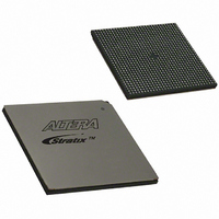
EP1S40B956C5
Manufacturer Part Number
EP1S40B956C5
Description
IC STRATIX FPGA 40K LE 956-BGA
Manufacturer
Altera
Series
Stratix®r
Datasheet
1.EP1S10F484I6N.pdf
(864 pages)
Specifications of EP1S40B956C5
Number Of Logic Elements/cells
41250
Number Of Labs/clbs
4125
Total Ram Bits
3423744
Number Of I /o
683
Voltage - Supply
1.425 V ~ 1.575 V
Mounting Type
Surface Mount
Operating Temperature
0°C ~ 85°C
Package / Case
956-BGA
Lead Free Status / RoHS Status
Contains lead / RoHS non-compliant
Number Of Gates
-
Available stocks
Company
Part Number
Manufacturer
Quantity
Price

Part Number:
EP1S40B956C5
Manufacturer:
ALTERA/阿尔特拉
Quantity:
20 000


1.5-V Regulator Application Examples
14–20
Stratix Device Handbook, Volume 2
Output voltage requirements
Supply voltages
Supply variance from Linear Technology data sheet
Estimated I
Estimated I
Total user-mode current consumption
Table 14–8. Voltage Regulator Selection Process for EP1C12F324C Design (Part 1 of 2)
Use Cyclone Power Calculator
Use Cyclone Power Calculator (not applicable in this example
because V
I
C C
= I
C C I N T
C C I N T
C C I O
C C I O
+ I
if regulator powers V
C C I O
= 3.3 V)
Synchronous Switching Regulator Example
This example shows a worst-case scenario for power consumption where
the design uses all the LEs and RAM.
requirements for 1.5-V design using a Cyclone EP1C12 FPGA.
Table 14–8
voltage regulator.
Output voltage precision requirement
Supply voltages available on the board
Voltage supply output current available for this
section (I
Variance of board supply (V
f
Average tog
Average tog
Utilization
Output and bidirectional pins
V
V
Efficiency
MAX
Table 14–7. Design Requirements for the Example EP1C12F324C
CCIO
CCINT
supply level
supply level
C C I O
I N , D C ( M A X )
uses the checklist on
IO
LC
Design Requirement
)
IN
)
page 14–9
Table 14–7
Supply variance = ±5%
to help select the appropriate
V
IN
shows the design
OR V
3.3 V
2 A
150 MHz
12.5%
12.5%
100%
125
3.3 V
1.5 V
5%
5%
90%
I
CCINT
V
I
CCIO
OUT
I
C C
CC
Altera Corporation
= 1.5 V
= 3.3 V
= 620 mA
= N/A
= 620 mA
Value
January 2005
Related parts for EP1S40B956C5
Image
Part Number
Description
Manufacturer
Datasheet
Request
R

Part Number:
Description:
CYCLONE II STARTER KIT EP2C20N
Manufacturer:
Altera
Datasheet:


Part Number:
Description:
CPLD, EP610 Family, ECMOS Process, 300 Gates, 16 Macro Cells, 16 Reg., 16 User I/Os, 5V Supply, 35 Speed Grade, 24DIP
Manufacturer:
Altera Corporation
Datasheet:
Part Number:
Description:
CPLD, EP610 Family, ECMOS Process, 300 Gates, 16 Macro Cells, 16 Reg., 16 User I/Os, 5V Supply, 15 Speed Grade, 24DIP
Manufacturer:
Altera Corporation
Datasheet:
Part Number:
Description:
Manufacturer:
Altera Corporation
Datasheet:
Part Number:
Description:
CPLD, EP610 Family, ECMOS Process, 300 Gates, 16 Macro Cells, 16 Reg., 16 User I/Os, 5V Supply, 30 Speed Grade, 24DIP
Manufacturer:
Altera Corporation
Datasheet:
Part Number:
Description:
High-performance, low-power erasable programmable logic devices with 8 macrocells, 10ns
Manufacturer:
Altera Corporation
Datasheet:
Part Number:
Description:
High-performance, low-power erasable programmable logic devices with 8 macrocells, 7ns
Manufacturer:
Altera Corporation
Datasheet:
Part Number:
Description:
Classic EPLD
Manufacturer:
Altera Corporation
Datasheet:
Part Number:
Description:
High-performance, low-power erasable programmable logic devices with 8 macrocells, 10ns
Manufacturer:
Altera Corporation
Datasheet:
Part Number:
Description:
Manufacturer:
Altera Corporation
Datasheet:
Part Number:
Description:
Manufacturer:
Altera Corporation
Datasheet:
Part Number:
Description:
Manufacturer:
Altera Corporation
Datasheet:
Part Number:
Description:
CPLD, EP610 Family, ECMOS Process, 300 Gates, 16 Macro Cells, 16 Reg., 16 User I/Os, 5V Supply, 25 Speed Grade, 24DIP
Manufacturer:
Altera Corporation
Datasheet: