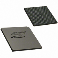
EP1S40B956C5 Altera, EP1S40B956C5 Datasheet - Page 412

EP1S40B956C5
Manufacturer Part Number
EP1S40B956C5
Description
IC STRATIX FPGA 40K LE 956-BGA
Manufacturer
Altera
Series
Stratix®r
Datasheet
1.EP1S10F484I6N.pdf
(864 pages)
Specifications of EP1S40B956C5
Number Of Logic Elements/cells
41250
Number Of Labs/clbs
4125
Total Ram Bits
3423744
Number Of I /o
683
Voltage - Supply
1.425 V ~ 1.575 V
Mounting Type
Surface Mount
Operating Temperature
0°C ~ 85°C
Package / Case
956-BGA
Lead Free Status / RoHS Status
Contains lead / RoHS non-compliant
Number Of Gates
-
Available stocks
Company
Part Number
Manufacturer
Quantity
Price
Part Number:
EP1S40B956C5
Manufacturer:
ALTERA/阿尔特拉
Quantity:
20 000
- Current page: 412 of 864
- Download datasheet (11Mb)
DDR Memory Support Overview
3–16
Stratix Device Handbook, Volume 2
f
bottom of the device. The phase-shift circuitry cannot be fed from other
sources such as the LE or the PLL internal output clocks. This phase-shift
circuitry is used for DDR SDRAM and RLDRAM II interfaces. For best
performance, turn off the input reference clock to the DQS phase-shift
circuitry when reading from the DDR SDRAM or RLDRAM II. This is to
avoid any DLL jitter incorrectly shifting the DQS signal while the FPGA
is capturing data.
1
A compensated delay element on each DQS pin allows for either a 90° or
a 72° phase shift, which automatically centers input DQS signals with the
data valid window of their corresponding DQ data signals. The DQS
signals drive a local DQS bus within the top and bottom I/O banks. This
DQS bus is an additional resource to the I/O clocks and clocks DQ input
registers with the DQS signal.
Refer to the DC & Switching Characteristics chapter in volume 1 of the
Stratix Device Handbook for frequency limits regarding the 72 and 90°
phase shift for DQS.
The phase-shifting reference circuit on the top of the device controls the
compensated delay elements for all 10 DQS pins located at the top of the
device. The phase-shifting reference circuit on the bottom of the device
controls the compensated delay elements for all 10 DQS pins located on
the bottom of the device. All 10 delay elements (DQS signals) on either the
top or bottom of the device shift by the same degree amount. For
example, all 10 DQS pins on the top of the device can be shifted by 90° and
all 10 DQS pins on the bottom of the device can be shifted by 72°. The
reference circuit requires a maximum of 256 system reference clock cycles
to set the correct phase on the DQS delay elements.
1
Figure 3–8
delay shift on the top of the device. This same circuit is duplicated on the
bottom of the device.
The I/O pins in I/O banks 1, 2, 5, and 6 can interface with the
DDR SDRAM at up to 150 MHz. See AN 342: Interfacing DDR
SDRAM with Stratix & Stratix GX Devices.
This applies only to the initial phase calculation. Altera
recommends that you enable the DLL during the refresh cycle of
the DDR SDRAM. Enabling the DLL for the duration of the
minimum refresh time is sufficient for recalculating the phase
shift.
shows the phase-shift reference circuit control of each DQS
Altera Corporation
June 2006
Related parts for EP1S40B956C5
Image
Part Number
Description
Manufacturer
Datasheet
Request
R

Part Number:
Description:
CYCLONE II STARTER KIT EP2C20N
Manufacturer:
Altera
Datasheet:

Part Number:
Description:
CPLD, EP610 Family, ECMOS Process, 300 Gates, 16 Macro Cells, 16 Reg., 16 User I/Os, 5V Supply, 35 Speed Grade, 24DIP
Manufacturer:
Altera Corporation
Datasheet:

Part Number:
Description:
CPLD, EP610 Family, ECMOS Process, 300 Gates, 16 Macro Cells, 16 Reg., 16 User I/Os, 5V Supply, 15 Speed Grade, 24DIP
Manufacturer:
Altera Corporation
Datasheet:

Part Number:
Description:
Manufacturer:
Altera Corporation
Datasheet:

Part Number:
Description:
CPLD, EP610 Family, ECMOS Process, 300 Gates, 16 Macro Cells, 16 Reg., 16 User I/Os, 5V Supply, 30 Speed Grade, 24DIP
Manufacturer:
Altera Corporation
Datasheet:

Part Number:
Description:
High-performance, low-power erasable programmable logic devices with 8 macrocells, 10ns
Manufacturer:
Altera Corporation
Datasheet:

Part Number:
Description:
High-performance, low-power erasable programmable logic devices with 8 macrocells, 7ns
Manufacturer:
Altera Corporation
Datasheet:

Part Number:
Description:
Classic EPLD
Manufacturer:
Altera Corporation
Datasheet:

Part Number:
Description:
High-performance, low-power erasable programmable logic devices with 8 macrocells, 10ns
Manufacturer:
Altera Corporation
Datasheet:

Part Number:
Description:
Manufacturer:
Altera Corporation
Datasheet:

Part Number:
Description:
Manufacturer:
Altera Corporation
Datasheet:

Part Number:
Description:
Manufacturer:
Altera Corporation
Datasheet:

Part Number:
Description:
CPLD, EP610 Family, ECMOS Process, 300 Gates, 16 Macro Cells, 16 Reg., 16 User I/Os, 5V Supply, 25 Speed Grade, 24DIP
Manufacturer:
Altera Corporation
Datasheet:


