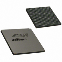
EP1S40B956C5 Altera, EP1S40B956C5 Datasheet - Page 358

EP1S40B956C5
Manufacturer Part Number
EP1S40B956C5
Description
IC STRATIX FPGA 40K LE 956-BGA
Manufacturer
Altera
Series
Stratix®r
Datasheet
1.EP1S10F484I6N.pdf
(864 pages)
Specifications of EP1S40B956C5
Number Of Logic Elements/cells
41250
Number Of Labs/clbs
4125
Total Ram Bits
3423744
Number Of I /o
683
Voltage - Supply
1.425 V ~ 1.575 V
Mounting Type
Surface Mount
Operating Temperature
0°C ~ 85°C
Package / Case
956-BGA
Lead Free Status / RoHS Status
Contains lead / RoHS non-compliant
Number Of Gates
-
Available stocks
Company
Part Number
Manufacturer
Quantity
Price
Part Number:
EP1S40B956C5
Manufacturer:
ALTERA/阿尔特拉
Quantity:
20 000
- Current page: 358 of 864
- Download datasheet (11Mb)
Clocking
Figure 1–21. Global & Regional Clock Connections from Side Clock Pins & Fast PLL Outputs
Notes to
(1)
(2)
1–48
Stratix Device Handbook, Volume 2
FPLL7CLK
FPLL8CLK
The global or regional clocks in a fast PLL’s quadrant can drive the fast PLL input. A dedicated pin or other PLL
must drive the global or regional source. The source cannot be driven by internally generated logic before driving
the fast PLL.
PLLs 3, 4, 9, and 10 are used for the HSSI block in Stratix GX devices and are not available for this use.
CLK2
CLK3
CLK0
CLK1
Figures
1–21:
PLL 7
PLL 1
PLL 2
PLL 8
g0
g0
g0
g0
l0
l1
l0
l1
l0
l1
l0
l1
2
When using a fast PLL to compensate for clock delays to drive logic on
the chip, the clock delay from the input pin to the clock input port of the
PLL is compensated only if the clock is fed by the dedicated input pin
closest to the PLL. If the fast PLL gets its input clock from a global or
regional clock or from another dedicated clock pin, which does not
directly feed the fast PLL, the clock signal is first routed onto a global
clock network. The signal then drives into the PLL. In this case, the clock
delay is not fully compensated and the delay compensation is equal to the
clock delay from the dedicated clock pin closest to the PLL to the clock
input port of the PLL.
For example, if you use CLK0 to feed PLL 7, the input clock path delay is
not fully compensated, but if FPLL7CLK feeds PLL 7, the input clock path
delay is fully compensated.
Figure 1–22
connections from the fast PLLs.
information as
each specific PLL output port drives to.
Regional
Clocks
shows the global and regional clock input and output
Tables 1–15
Clocks
Global
and
1–16
Figure 1–22
Regional
Clocks
but with the added detail of where
shows graphically the same
2
l0
l1
g0
l0
l1
g0
l0
l1
g0
l0
l1
g0
PLL 10
PLL 4
PLL 3
PLL 9
Altera Corporation
July 2005
FPLL10CLK
CLK10
CLK11
CLK8
CLK9
FPLL9CLK
Related parts for EP1S40B956C5
Image
Part Number
Description
Manufacturer
Datasheet
Request
R

Part Number:
Description:
CYCLONE II STARTER KIT EP2C20N
Manufacturer:
Altera
Datasheet:

Part Number:
Description:
CPLD, EP610 Family, ECMOS Process, 300 Gates, 16 Macro Cells, 16 Reg., 16 User I/Os, 5V Supply, 35 Speed Grade, 24DIP
Manufacturer:
Altera Corporation
Datasheet:

Part Number:
Description:
CPLD, EP610 Family, ECMOS Process, 300 Gates, 16 Macro Cells, 16 Reg., 16 User I/Os, 5V Supply, 15 Speed Grade, 24DIP
Manufacturer:
Altera Corporation
Datasheet:

Part Number:
Description:
Manufacturer:
Altera Corporation
Datasheet:

Part Number:
Description:
CPLD, EP610 Family, ECMOS Process, 300 Gates, 16 Macro Cells, 16 Reg., 16 User I/Os, 5V Supply, 30 Speed Grade, 24DIP
Manufacturer:
Altera Corporation
Datasheet:

Part Number:
Description:
High-performance, low-power erasable programmable logic devices with 8 macrocells, 10ns
Manufacturer:
Altera Corporation
Datasheet:

Part Number:
Description:
High-performance, low-power erasable programmable logic devices with 8 macrocells, 7ns
Manufacturer:
Altera Corporation
Datasheet:

Part Number:
Description:
Classic EPLD
Manufacturer:
Altera Corporation
Datasheet:

Part Number:
Description:
High-performance, low-power erasable programmable logic devices with 8 macrocells, 10ns
Manufacturer:
Altera Corporation
Datasheet:

Part Number:
Description:
Manufacturer:
Altera Corporation
Datasheet:

Part Number:
Description:
Manufacturer:
Altera Corporation
Datasheet:

Part Number:
Description:
Manufacturer:
Altera Corporation
Datasheet:

Part Number:
Description:
CPLD, EP610 Family, ECMOS Process, 300 Gates, 16 Macro Cells, 16 Reg., 16 User I/Os, 5V Supply, 25 Speed Grade, 24DIP
Manufacturer:
Altera Corporation
Datasheet:


